
PCB assembly means putting parts on a circuit board. This makes devices that we use every day, like phones and medical tools. By 2025, this process will be even more important. People want faster, smaller, and better electronics. 5G technology and HDI PCBs help make devices faster and smarter. These can handle more data and do more tasks. The PCB market might grow to $80.9 billion by 2024. This shows how important it is becoming. Using eco-friendly methods and new materials will also change PCB assembly in the future.
Key Takeaways
PCB assembly is important for making electronic devices work. It makes sure parts are in the right place and connected properly.
Robots and machines are changing how PCB assembly is done. They make it faster and more accurate, helping to create better electronics.
Being eco-friendly is now very important in PCB assembly. Using green materials and methods helps the Earth and attracts buyers who care about the environment.
HDI PCBs are important for modern gadgets. They make smaller and stronger devices, which people want today.
Checking quality is very important in PCB assembly. Using smart testing tools makes products reliable and earns customer trust.
What is PCB Assembly?
Definition and Purpose of PCB Assembly
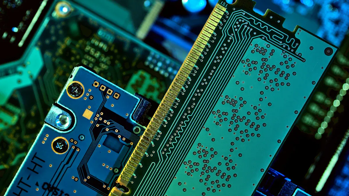
PCB assembly means putting electronic parts on a circuit board. This changes a plain board into a working circuit board. The steps include adding solder paste, placing parts, and soldering them. These steps make sure the board works in devices.
The goal of PCB assembly is to make a strong base for parts to work together. Rules like IPC J-STD-001 and IPC-A-620 guide how to do this well. For example:
Standard | Purpose |
|---|---|
IPC J-STD-001 | Makes sure soldering is done well for good performance. |
IPC-A-620 | Sets rules for making cable and wire setups. |
IPC-6012 | Explains how strong rigid circuit boards should be. |
IPC-6013 | Focuses on flexible boards and their special uses. |
By following these rules, makers ensure PCB assembly fits modern tech needs.
Difference Between PCB Assembly and PCB Manufacturing
PCB assembly and PCB manufacturing are different but connected. PCB manufacturing makes the board with its layers and pads. PCB assembly adds parts to the board to make it work.
The difficulty and cost depend on the board’s layers and use. For example:
Layer Count | Complexity | Cost Impact | Typical Applications |
|---|---|---|---|
Single Layer | Simple | Low | Basic devices like calculators. |
Double Layer | Easy | Low to Medium | Everyday items like remote controls. |
4 Layer | Medium | Medium | Industrial tools and advanced gadgets. |
6 Layer | Harder | Medium to High | Telecom devices and smart gadgets. |
8+ Layer | Most Complex | High | Fast data systems and supercomputers. |
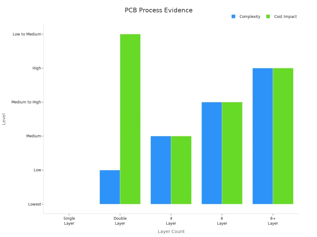
PCB manufacturing builds the board, while PCB assembly adds life to it. Together, they make modern electronics possible.
Importance of PCB Assembly in Electronics
PCB assembly is very important for electronics. It makes sure parts are placed and connected right. This helps devices work as they should. Without good assembly, even great designs would fail.
It also saves money and adds flexibility. New methods like robot soldering and part placement lower costs and improve accuracy. These help make high-quality devices faster.
PCB assembly also helps create new technology. It allows for small, powerful devices like phones and medical tools. By using smart designs and advanced methods, makers meet the need for better, faster, and smarter tech.
The PCB Assembly Process
Key Steps in PCB Assembly
The PCB assembly process has important steps to make a working circuit board. These steps help ensure the board works well and lasts long. Here’s a simple breakdown:
Research and Planning: Study the market and check patents to follow industry rules.
Design Development: Write a plan for the product and analyze design needs.
Layer Alignment and Inspection: Match layers using holes and check for mistakes with cameras.
Layer Bonding: Stick layers together with special sheets and pressure.
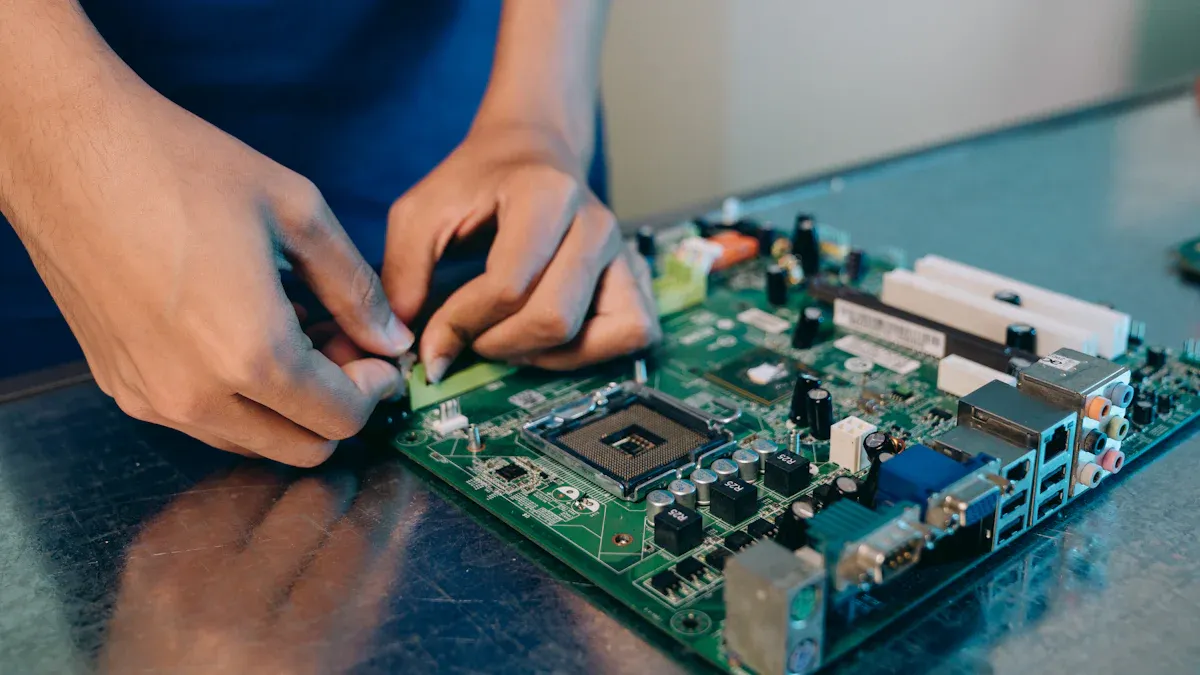
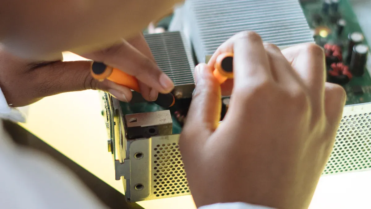
Drilling and Component Placement: Drill holes and place parts using machines for accuracy.
Each step is important to make sure the PCB works correctly and meets quality standards.
Surface Mount vs. Through-Hole Assembly
There are two main ways to attach parts to a PCB: surface mount and through-hole assembly. Through-hole assembly makes strong connections, so it’s good for tough devices and ones that handle heat. It’s often used in factory machines and power tools. Surface mount assembly is faster and saves space. It lets parts sit close together, which reduces signal problems. This method is great for small devices like phones and laptops because it’s cheaper and works well with machines. Choosing between these methods depends on what your device needs, like strength, size, or how many you’ll make.
Role of PCB Design and Assembly in Device Functionality
How a PCB is designed and assembled affects how well devices work. Important things to focus on include:
Logical Component Placement: Keeps signal paths short for better performance.
Efficient Routing: Stops signals from interfering with each other.
Solid Ground and Power Planes: Makes signals clear and reduces noise.
Thermal Management: Stops overheating to keep devices stable.
Impedance Management: Keeps signals steady for reliable use.
By paying attention to these details, you can make PCBs that support new technology and meet today’s electronic needs.
Technologies and Materials in PCB Assembly
Essential Materials for PCB Assembly
The materials used in circuit boards are very important. They affect how well the board works and lasts. Substrates like FR-4, CEM-1, and ceramic give support and insulation. FR-4 is strong and cheap, so it’s used a lot. CEM-1 is cheaper and works for simple devices. Ceramic is great for high-heat environments.
Copper is the main material for carrying electricity in circuit boards. It’s very good at conducting electricity, so it’s perfect for circuits. For special uses, makers use epoxy resins for fast signals or aluminum for heat control. These materials help circuit boards meet the needs of modern gadgets.
Tools and Equipment Used in PCB Assembly
Making circuit boards needs special tools to work well. Pick-and-place machines put parts on boards quickly and correctly. Soldering tools, like reflow ovens, connect parts to the board strongly.
Inspection tools check for mistakes during assembly. AOI systems use cameras to find missing or wrong parts. X-ray machines look at hidden connections. These tools make sure the board is good before it’s sold.
Quality Control in PCB Assembly
Quality checks make sure circuit boards work as they should. First, workers look for obvious problems. Then, automated tests check if the board works right. Functional tests confirm the board can do its job. These steps stop bad products from being sold.
Inspection Stage | What It Does | Standards Used |
|---|---|---|
Pre-production | Checks design and specs before assembly starts. | ISO 9001:2015 |
Production | Watches assembly to catch problems early. | IPC A-610 |
Pre-shipment Inspection | Final check to ensure quality before shipping. | IPC A-610 |
Container Loading Supervision | Makes sure products are packed safely for transport. | ISO 9001:2015 |
Following these steps makes sure circuit boards are reliable and high-quality. Good quality control saves money and earns customer trust.
Trends Shaping PCB Assembly in 2025
Automation and Robotics in PCB Assembly
Automation and robots are changing how electronics are made. By 2025, these tools will make PCB assembly faster and cheaper. Robots can do jobs like soldering and placing parts better than people. In 2023, there were over 3.5 million robots working worldwide. Industries like electronics, cars, and medicine are using robots the most.
Assembly lines are key to this change. In 2023, they were the biggest part of the automation market. Automated lines help make more products with fewer mistakes. This is especially useful for making electronics quickly and with good quality.
Automation also works with Industry 4.0. This uses AI, big data, and robots to improve factories. For example, AI can find problems early so they don’t cause delays. This helps meet the growing need for high-quality PCBs.
Sustainability and Eco-Friendly Practices
Making PCBs is becoming more eco-friendly. As people care more about the planet, companies must follow green rules. Laws like RoHS and REACH limit harmful materials in electronics. The WEEE Directive makes companies recycle old products properly.
Regulation | What It Does |
|---|---|
Tracks and reports harmful waste. | |
RoHS | Limits harmful materials in electronics. |
REACH | Promotes safer chemicals in products. |
WEEE Directive | Requires recycling and safe disposal of old electronics. |
Eco-friendly steps include cutting waste and using better materials. Tracking waste helps find ways to improve. Using lead-free solder and biodegradable parts lowers harm to the planet.
Being eco-friendly helps the Earth and boosts your brand. People like buying from companies that care about the environment. This gives you an edge in the market.
Miniaturization and High-Density PCB Designs
Smaller, stronger devices are driving new PCB designs. High-Density Interconnect (HDI) PCBs are leading this trend. They pack more circuits into smaller spaces using special techniques like microvias and blind vias. This allows small designs without losing features.
HDI PCBs are vital for industries like electronics and aerospace. They save space and weight, making them perfect for phones, wearables, and drones. But making HDI PCBs needs advanced tools and skilled workers, which limits who can make them.
HDI PCBs also have challenges. High circuit density can cause signal problems like crosstalk. Careful design and testing can fix these issues. This ensures small devices work well.
Trend | What It Means |
|---|---|
Smaller Electronics | People want tiny devices that still work well. |
Growth of IoT Devices | More connected devices need better PCB assembly solutions. |
Green Manufacturing | Companies are using safer materials and cutting waste. |
Automation and Industry 4.0 | AI and robots are making factories smarter and faster. |
Need for Custom Products | Different industries want PCBs made just for their needs. |
By focusing on miniaturization and HDI designs, you can stay ahead. These ideas meet what customers want and help create the next wave of cool gadgets.
Innovations in Testing and Inspection Technologies
Testing tools have changed how we check PCB quality. These new tools find mistakes early, save time, and ensure products meet high standards. Using modern inspection methods helps make reliable and strong electronics.
Automated Optical Inspection (AOI)
Automated Optical Inspection (AOI) is key in PCB assembly today. It uses cameras and smart software to check boards during production. AOI can inspect bare PCBs to match design plans before assembly starts. During assembly, it checks if parts are placed right and soldered well, making sure the board works properly.
AOI finds common problems like:
Missing or misplaced parts.
Parts facing the wrong way.
Solder issues like too little solder or solder bridges.
PCB damage, like broken traces or dirt on the board.
Adding AOI to your process helps catch these problems early and avoids costly fixes later.
First Article Inspection (FAI)
First Article Inspection (FAI) is another important step in PCB assembly. It checks if your production process makes PCBs that meet design rules. FAI proves that all design and quality needs are checked and recorded. This is especially helpful at the start of production when mistakes can cause big problems.
With FAI, you can:
Make sure your assembly process meets quality rules.
Spot and fix problems before making many boards.
Ensure your PCBs match customer needs and follow rules.
This careful checking keeps your products consistent and trustworthy.
Advanced Testing Techniques
Modern testing goes beyond just looking at boards. Functional tests check if the PCB works in real-life situations. For example, in-circuit testing (ICT) tests each part’s electrical performance. Boundary scan testing finds connection problems in complex circuits.
These advanced tests help you:
Confirm your PCB works before selling it.
Find hidden problems not seen in visual checks.
Make your electronics more reliable overall.
Benefits of Modern Testing and Inspection
New testing and inspection tools bring many benefits:
Better Accuracy: Machines reduce mistakes and give steady results.
Faster Production: Finding problems early avoids delays and speeds up work.
Lower Costs: Fixing issues early saves money and reduces waste.
Higher Quality: Careful checks ensure your PCBs are top-notch.
Using these tools helps you stay ahead in the electronics market. It also ensures you deliver products that customers trust and love.
Tip: Buying advanced testing tools improves your process and builds customer trust by ensuring your products are reliable and high-quality.
The Future of PCB Assembly
How PCB Assembly Drives Innovation
PCB design and assembly are key to creating new ideas. By using advanced tools like AI and IoT, devices become smarter and faster. For example, AI finds mistakes early and speeds up production. IoT connects devices, making them more useful and interactive.
The rise of 5G networks has increased the need for better PCBs. These boards allow faster data and improved device performance. Flexible PCBs are another big step forward. They help make smaller and more adaptable gadgets. These are important for wearables, medical tools, and compact tech.
Case Study | Description |
|---|---|
Automation challenges and solutions in flex PCB assembly drive innovation. | |
Paragon Robotics PCB Assembly | Full PCB assembly capabilities, including certifications, enhance innovation. |
These improvements show how PCB assembly helps create better electronics.
Challenges and Opportunities in PCB Assembly
The PCB industry has problems but also chances to grow. Complex designs need careful assembly, which can be tricky. Supply chain issues and higher material costs add to the struggles. But these problems push companies to find smart solutions.
Factor | Description |
|---|---|
Growth Drivers | Demand for connected vehicles, advanced systems, and reliable electronics. |
Challenges | Complex designs, supply chain issues, and cost concerns. |
Using automation and eco-friendly methods can solve these issues. For example, AI in assembly reduces mistakes and works faster. Green practices, like lead-free solder, meet rules and attract eco-friendly buyers.
The Role of PCB Assembly in Smart Technologies
Smart tech depends on good PCB assembly. Gadgets like smartwatches, home assistants, and self-driving cars need small, powerful PCBs. Flexible and HDI PCBs save space and improve how devices work.
Combining IoT and AI makes assembly and devices better. For instance, IoT sensors track real-time data to ensure quality. AI studies this data to stop problems before they happen.
3D printing is also changing PCB production. It allows quick prototypes and custom designs, helping meet unique needs. Using these tools keeps you ahead in the competitive tech world.
PCB assembly is crucial for making dependable and creative devices. It connects electronic parts so gadgets work properly every day. Without PCB assembly, today’s technology wouldn’t be possible.
New ideas like robots, green methods, and compact designs are solving 2025’s needs. These changes make production quicker, devices smaller, and manufacturing better for the planet.
Key Takeaway: PCB assembly is essential for building electronics. Using modern tools can create smarter and eco-friendly devices for the future.
FAQ
What is the difference between PCB assembly and PCB fabrication?
PCB assembly means adding and soldering parts to a circuit board. This makes the board work in devices. PCB fabrication is making the board itself with layers and pads. Think of fabrication as creating the board and assembly as making it work.
Why is automation important in PCB assembly?
Automation makes PCB assembly faster and more accurate. Machines do tasks like soldering and placing parts. This lowers mistakes and keeps quality steady. With automation, you can make better electronics quickly and for less money.
What are HDI PCBs, and why are they important?
High-Density Interconnect (HDI) PCBs fit more circuits in small spaces. They use special methods like microvias to do this. These boards are great for gadgets like phones and smartwatches. They save space, weigh less, and handle fast signals, making them ideal for modern devices.
How does sustainability impact PCB assembly?
Sustainability means cutting waste and using safer materials. Rules like RoHS and REACH stop harmful substances in PCBs. By going green, you help the planet, follow laws, and attract buyers who care about eco-friendly products.
What tools are essential for PCB assembly?
Important tools include pick-and-place machines for adding parts, reflow ovens for soldering, and inspection tools like AOI and X-ray machines. These tools help make sure boards are built right. Using good equipment makes strong and reliable circuit boards.
Tip: Buying better tools and using green methods can improve your PCB assembly and build customer trust.
See Also
Understanding PCBA Manufacturing and Its Importance in Industry
The Significance of PCB Design in Electronic Devices Explained
Exploring PCBA Services and Their Role in Electronics Production
Defining Turnkey PCB Assembly and Its Importance in Manufacturing