
When you put together a pcb board with surface mount parts, you must watch every step closely. Being careful during pcb board assembly stops problems like solder bridging, tombstoning, or putting parts in the wrong place. Many people run into these problems when doing diy pcb assembly:
Solder bridging or short circuits
Not enough solder on joints
Tombstoning of parts
Solder balling and beading
You can stop these problems if you follow each step in the pcb assembly process. Hobbyists may take up to a minute to place each part, but professionals are much quicker. Go slowly and check your work to get the best results.
Key Takeaways
Look over your design files closely before you start. This helps you avoid mistakes and saves time. Keep your workspace neat and tidy. Use the right tools to make fewer errors. Put solder paste on evenly with a stencil. This stops problems like solder bridging. Place parts carefully with tweezers or machines. Check their position and direction again. Watch the reflow soldering temperature closely. This makes strong solder joints and stops defects.
PCB Board Assembly Preparation
Design File Verification
Before you start pcb board assembly, you need to check your design files carefully. This step helps you avoid mistakes and saves time later. You should follow these steps:
Review your CAD files. These files show the 2D and 3D models for your printed circuit board design.
Check your Gerber files. These files show the layout of copper layers, solder mask, and silkscreen.
Look at your Bill of Materials (BOM). Make sure every part number matches the description and quantity. Each part should have a reference designator so you know where it goes.
Confirm your pick and place files. These files show the exact spot and angle for each component.
Verify solder paste files. These files tell you where and how much solder paste to apply.
Use assembly drawings and schematics. These help you see where each part goes and how everything connects.
Make sure your drill files are correct. They show where holes go and what size they need to be.
Tip: Double-check that all files match your latest design changes. Missing or wrong information can cause delays during circuit board assembly.
Workspace and Tools Setup
A clean and organized workspace helps you build your pcb board assembly with fewer errors. You should gather all your tools before you begin. Here is a list of important tools and equipment:
Flush cutters for trimming leads.
Wire strippers for preparing wires.
Magnifying glass or microscope (10x or higher) for checking small solder joints.
Digital multimeter for testing connections.
ESD-safe wrist strap and mat to protect parts from static electricity.
Soldering fume extractor to keep the air clean.
Good lighting, such as desk lamps or ring lights.
You should also keep your workspace at a stable temperature and humidity. Store your boards and parts in dry packs with desiccants to prevent moisture damage. Always handle boards by the edges and avoid touching metal areas. Use ESD-safe tools and mats to protect sensitive components.
Note: Organize your components and prepare your solder paste and stencil before you start. This makes the assembly process smoother and helps you avoid mistakes.
Solder Paste Application
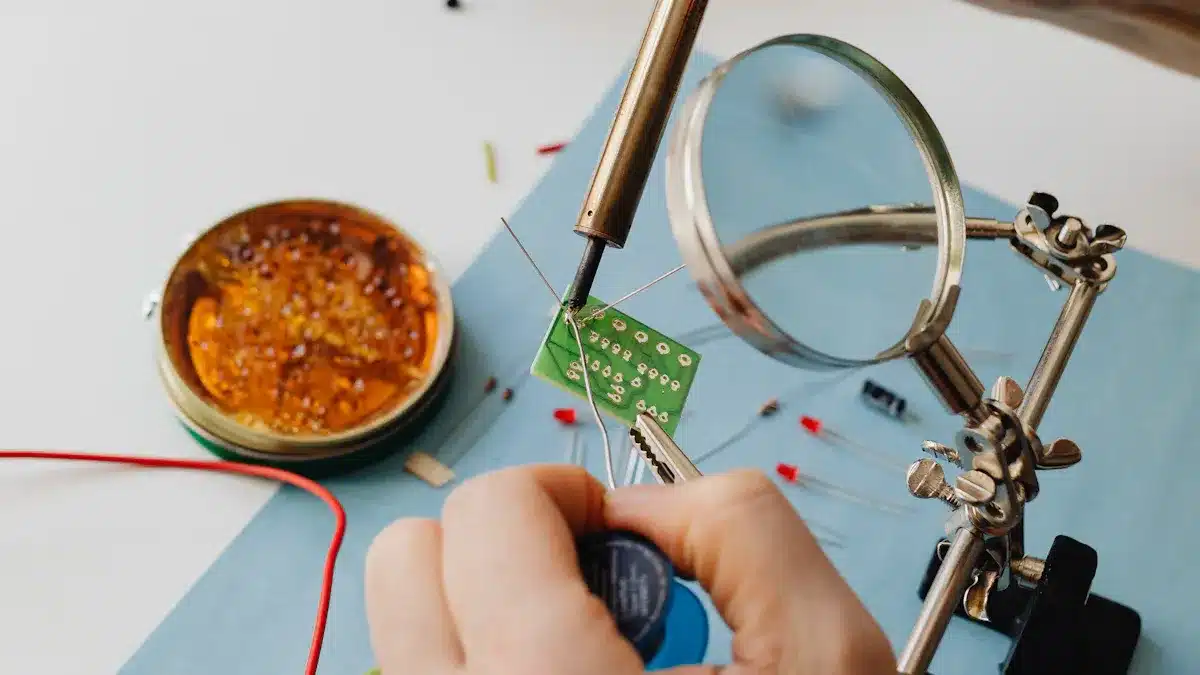
Putting solder paste on the board is very important. You must put the right amount on each pad. This stops problems when you solder and keeps surface mount parts in place.
Stencil Use
There are two main ways to put on solder paste. You can use a syringe or a stencil. Most people pick a stencil because it is faster and more exact. Stencils have tiny holes that match the pads on your PCB. You line up the stencil with the board using special marks. Then, you spread the solder paste over the stencil with a squeegee. Hold the squeegee at a 45-degree angle. The stencil makes sure each pad gets the right amount of solder paste. This way, you get even solder on every pad. It also helps stop mistakes like solder bridging or weak joints.
Stencils are made from stainless steel. This makes them strong and helps the paste come off smoothly.
Step stencils let you use different amounts of solder paste for different parts.
The right stencil thickness helps you get good solder joints every time.
Laser cutting and polishing make the holes better and lower solder problems.
Tip: Always check if your stencil lines up before you start. Good alignment keeps the solder paste on the pads.
Common Mistakes
Many beginners make mistakes with solder paste. You can stop most problems if you know what to look for. Here is a table that shows common mistakes, why they happen, and how to stop them:
Mistake | Causes | Impact | Prevention Strategies |
|---|---|---|---|
Solder Bridging | Too much solder paste, poor alignment | Short circuits | Use correct stencil, align carefully |
Solder Balls | Moisture, wrong reflow profile | Unreliable connections | Store paste properly, control heating |
Insufficient Solder | Not enough paste, damaged stencil | Weak solder joints | Check stencil, use fresh paste |
Stencil Clogging | Dirty stencil, old paste | Missing solder deposits | Clean stencil, use quality paste |
Misalignment | Vibration, poor setup | Open circuits | Stabilize equipment, inspect alignment |
Always use the right amount of solder paste. Work fast so the paste does not dry out. Watch the heat when you solder so you do not hurt the parts. Clean your tools after you finish to keep them nice. Practice on old boards to get better at soldering.
Assemble a PCB: Component Placement
Manual vs. Machine Placement
When you start placing components on your PCB, you can choose between manual and machine placement. Each method has its own strengths and weaknesses.
Manual placement depends on your skill and attention. You use tweezers or a vacuum tool to pick up each part and set it on the board. This method works well for prototypes or small batches. You can spot design errors and make changes quickly. Manual assembly gives you more control and flexibility, especially if you work with special or odd-shaped parts. However, manual placement is slower and less accurate. You may find it hard to place very small parts, like 1005 size chips or fine-pitch ICs. Mistakes can happen, such as mixing up parts or putting them in the wrong direction. The quality of your work can change from board to board.
Automatic placement machines use advanced technology to place parts quickly and with high precision. These machines use cameras and software to line up each part perfectly. They can place thousands of parts per hour, making them ideal for large production runs. Machine placement gives you consistent results and fewer errors. You can trust the machine to handle tiny parts and complex chips, like BGAs and CSPs, with accuracy as fine as 50 micrometers. This level of precision is hard to match by hand.
Here is a table that compares manual and automated placement:
Aspect | Manual Placement | Machine Placement |
|---|---|---|
Speed | Slow | Very fast |
Accuracy | Depends on operator | High, consistent |
Flexibility | Easy to change or fix | Harder to change once set up |
Cost | Low for small batches | High setup cost, low per unit for large runs |
Suitability | Prototypes, special parts | Mass production, tiny or complex parts |
Error Rate | Higher, prone to human mistakes | Lower, fewer defects |
Tip: Use manual placement for small projects or when you need to make changes. Choose machine placement for high-volume jobs or when you need perfect accuracy.
Automatic machines also help keep your workspace safer. They reduce your exposure to fumes and sharp tools. For most hobbyists, manual placement is enough. If you want to build many boards or work with very small parts, consider using a pick-and-place machine.
Placing Small SMD Parts
Placing small SMD parts takes patience and practice. You need steady hands and the right tools. Follow these steps to get good results:
Pick up the part with tweezers or a vacuum tool. Hold it gently so you do not drop or damage it.
Bring the part close to the board. Lower it until it almost touches the solder paste.
Look at the pads through a magnifier or microscope. Make sure the leads line up with the pads.
Rotate the part if needed. Use your tool to get the right direction.
Set the part down on the solder paste. Press lightly to release it.
Let the sticky solder paste hold the part in place. Try not to move the board after this step.
If you see a small misalignment, do not worry. The reflow process will help center the part as the solder melts.
Avoid picking up and moving parts after you place them. If you must, use tweezers and add more solder paste if needed.
Keep all resistors and capacitors facing the same way. This makes troubleshooting and reading values easier.
Check your solder paste under a microscope. Make sure it covers the pads but does not touch other pads.
If you see solder bridging, use flux and copper wick to clean it up.
Rest your hand on the table to keep it steady while placing components.
If you have access to a pick-and-place machine, use it for better speed and accuracy.
Try low-temperature solder paste if you want an easier reflow process.
Note: Most errors during placing components come from misalignment, wrong orientation, or using the wrong footprint. Always check datasheets and make sure your parts match the board layout.
You should also leave enough space between parts. For small chips, keep at least 6 mils between them. For sensitive parts like BGAs, use 39 mils. Place connectors and large parts at least 20 mils apart. Keep all parts 50-75 mils from the board edge to avoid damage. Solder mask dams of about 1.6 mils help prevent solder bridging.
If you follow these steps, you will reduce mistakes like tombstoning, solder bridging, or open circuits. Careful placing components helps your board work as planned and makes later steps easier.
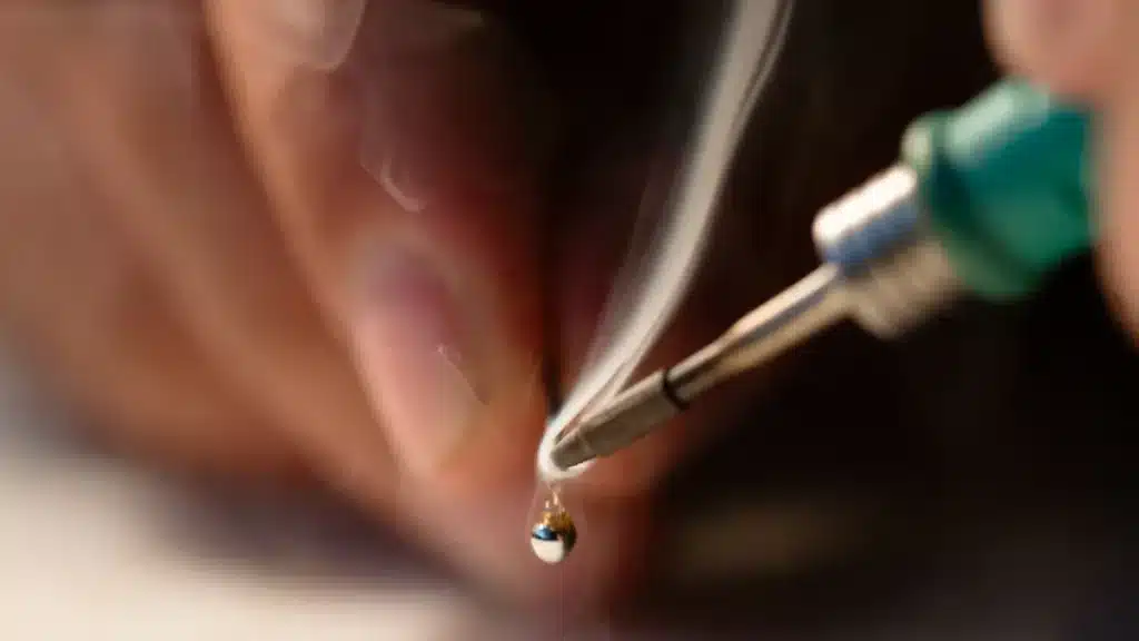
Reflow Soldering
Reflow soldering melts the solder paste. This makes strong electrical connections on your PCB. You must watch the temperature closely during this step. Good temperature control keeps your board and parts safe. It also helps you get strong solder joints.
Temperature Profile
You need to use a special temperature plan in a reflow oven. This plan has four main zones. Each zone has its own job and temperature range. If you follow these steps, your soldering will work well:
Preheat Zone
First, heat the board slowly. This wakes up the flux in the solder paste. It also stops the board from getting shocked by heat.Temperature: 25°C to 150°C for leaded solder, up to 180°C for lead-free solder
Duration: 60 to 90 seconds
Heating Rate: 1.5°C to 3°C per second
Purpose: Dry out solvents, start the flux, and stop splatter
Soak Zone
Keep the temperature steady for a while. This lets the flux clean the metal pads. It also helps the whole board get the same heat.Temperature: 150°C to 200°C for leaded, 180°C to 220°C for lead-free
Duration: 60 to 120 seconds
Purpose: Remove oxides and get ready for soldering
Reflow Zone
Heat the board above the solder’s melting point. The solder paste melts and makes the joints.Temperature: 210°C to 240°C for leaded, 240°C to 260°C for lead-free
Peak Temperature: 20°C to 40°C hotter than the solder’s melting point
Time Above Liquidus: 30 to 60 seconds
Purpose: Make sure the solder flows and forms good joints
Cooling Zone
Cool the board down at a steady speed. This hardens the solder and stops problems.Cooling Rate: 2°C to 4°C per second for lead-free solder
Duration: 30 to 60 seconds
Purpose: Stop stress and keep joints from breaking
Tip: Use a thermocouple to check the heat in different places on your board. This helps you make sure the whole board heats up the right way.
You can pick different temperature plans, like Ramp-Soak-Spike or Ramp-to-Spike. The best plan depends on your solder paste, board size, and parts. Always look at the solder paste maker’s advice. If you use the wrong plan, you might get cold solder joints or broken parts.
Avoiding Solder Defects
Many things can go wrong during reflow soldering. You can stop most problems if you know what causes them and how to fix them. Here is a table that shows common solder problems, why they happen, and how to stop them:
Defect | Causes | Preventive Measures |
|---|---|---|
Solder Bridging | Too much solder paste, bad stencil, wrong reflow profile, misalignment | Use correct stencil, control paste, adjust profile, check placement |
Tombstoning | Uneven heating, pad size issues, not enough solder paste, placement | Balance heating, standardize pads, check paste, improve placement |
Solder Balling | Moisture in paste, too much paste, bad profile, dirty PCB | Store paste well, control amount, optimize profile, clean PCB |
Voids in Joints | Too much flux, low preheat, short time, contamination | Adjust process, control flux, avoid contamination |
Component Deviation | Placement machine issues, low paste viscosity, vibration | Calibrate machine, use thick paste, adjust speed |
Cracked Components | Thermal mismatch, high temperature, moisture, fast cooling | Use right curve, store parts well, control cooling |
Solder Joint Cracks | Mechanical damage, bad solder, slow cooling, poor wetting | Reduce vibration, use good solder, control cooling, improve wetting |
Tin Whiskers | Stress, pure tin coatings | Use alloy coatings, heat treat, use intermediate coatings |
If you use the right amount of solder paste and a good stencil, you can stop solder bridging. Keep your solder paste in a cool, dry place. Clean your PCB before you start soldering. Always check your reflow plan and change it if you see problems. If you cool the board too fast, you might get cracks in the solder. If you cool it too slowly, the solder can get weak.
Bad temperature control can cause lots of problems. Too much heat can hurt your parts or the PCB. You might see burnt spots, lifted pads, or melted plastic. Not enough heat can make cold solder joints. These joints look dull and do not work well. If you see solder splatter or bridges, you may have used too much heat. Always follow the temperature plan for your solder paste and parts.
Note: Good quality checks help you get more working boards. Look at your boards after soldering. Use tools like Automated Optical Inspection (AOI) to find problems early. If you keep making your process better, you will get better boards and waste less.
Inspection and Rework
Solder Joint Check
You need to check each solder joint after soldering. Careful checking helps you find problems early. This stops your board from failing later. You can use different ways to look for defects. Visual inspection works well for simple boards. You look for things like solder bridging, cold joints, or missing parts. For harder boards, you should use special tools.
Here is a table that shows how popular inspection methods work for solder joints:
Inspection Method | Key Features and Effectiveness for Solder Joint Defects | Advantages | Limitations |
|---|---|---|---|
Automated Optical Inspection (AOI) | Uses cameras and lights to spot visible defects like bridging or not enough solder | Fast, accurate, less human mistakes | Cannot check hidden joints under BGAs or crowded spots |
Automatic Laser Test (ALT) Measurement | Measures solder joint height and alignment with lasers, good for solder paste checks | Quick, detailed measurements for process control | Mostly for before assembly, can be affected by interference |
Uses X-rays to see hidden solder joints and inside defects | Finds voids, cracks, and hidden problems, does not damage the board | Costs a lot, needs skilled workers |
You can see how these methods work for finding solder joint problems in the chart below:
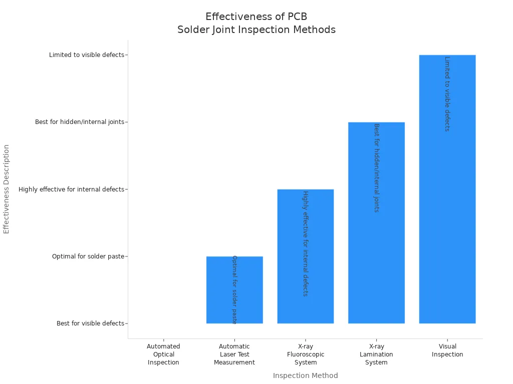
AOI is best for finding problems you can see. X-ray inspection finds hidden problems, like voids or cracks under BGAs. ALT helps you check solder paste before you put on parts.
Fixing Issues
If you find problems during inspection, you must fix them before moving on. First, get your workspace ready. Clean your area and make sure air can move well. Hold the PCB with holders and use ESD protection.
Follow these steps to fix soldering problems:
Check the board with a microscope or AOI system. Use X-ray inspection for hidden solder joints.
Take out bad parts. Use a hot air station at 300-350°C for surface mount parts. For through-hole parts, use a desoldering pump or braid.
Clean the pads with 99% isopropyl alcohol and a lint-free cloth. Remove old solder and flux.
Get the area ready by putting on fresh flux. Make sure pads are flat and clean.
Put new parts on with tweezers or a pick-and-place tool. Put solder paste on the pads.
Solder the new part with a hot air station or reflow oven. For small parts, touch up with a soldering iron.
Check the fixed solder joints with a microscope. Look for even joints and no voids.
Test the board for electrical continuity and resistance. Do a functional test to make sure it works right.
Example: If you need to take off a tombstoned 0603 resistor, heat it for 10-15 seconds with a 2mm nozzle before lifting it off.
Write down every step you do for fixing. Careful fixing and checking help you get strong solder joints and a working PCB board.
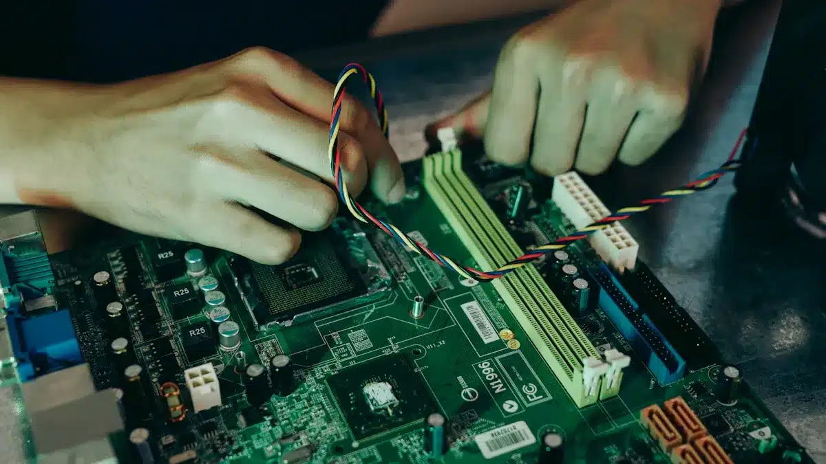
Assemble PCB Board: Through-Hole and Final Steps
Through-Hole Component Soldering
You often add through-hole parts after you finish surface mount assembly. These parts have leads that go through holes in the board. You use a soldering iron to heat the lead and the pad, then feed solder into the joint. This method gives strong mechanical support, which is important for connectors, switches, and heavy parts.
Here is a table that shows the main differences between through-hole and surface mount assembly:
Aspect | Through-Hole Assembly | Surface Mount Assembly |
|---|---|---|
Component Mounting | Insert leads into drilled holes, solder on the other side. | Mount directly on the PCB surface, solder to pads. |
Component Size | Larger components. | Smaller components, higher density. |
Assembly Process | Manual soldering, more time needed. | Automated process, faster and cheaper for large runs. |
Repairability | Easier to repair or replace by hand. | Needs special tools for repair. |
Reliability | Stronger mechanical support. | Less mechanical strength, but good for small devices. |
Space and Weight | Good for high power and strength. | Best for small, light, and complex boards. |
You should use through-hole soldering for parts that need extra strength or for prototypes you want to test and change.
Cleaning the Board
After you finish soldering, you need to clean the board. Cleaning removes flux residue, which can cause corrosion or electrical problems. You can use several methods:
Wipe the board with high-purity isopropyl alcohol (IPA) and a soft brush.
Use ultrasonic cleaning for boards with many parts or hard-to-reach spots.
Try automated cleaning systems for large batches.
Match the cleaning method to the type of flux you used. Rosin flux needs solvents, water-soluble flux needs deionized water, and no-clean flux may still need cleaning in harsh conditions.
Tip: Clean the board soon after soldering. This helps prevent sticky residue and keeps your board reliable.
Functional Testing
You must test your board before you finish the assemble pcb board process. Functional testing checks if your board works as planned. You can use these steps:
Power on the board and check for correct voltage.
Use a multimeter to test connections and signals.
Run load tests to see if the board works under real conditions.
Use in-circuit testing to check each part and connection.
Try burn-in testing for boards that need to work in tough environments.
If your board fails a test, follow these troubleshooting steps:
Check the board for soldering mistakes or misplaced parts.
Inspect for damaged or wrong components.
Use a multimeter or oscilloscope to find problems.
Test each part if needed.
Quality checks like visual inspection, AOI, and X-ray inspection help you find hidden problems. Careful testing and cleaning make sure your board is safe and ready to use.
You can get good at pcb board assembly if you follow each step carefully. First, check your files and make sure your workspace is ready. Put the components in the right spots and use the correct soldering methods. Always look over your work and fix any problems you see. To keep learning, read guides about SMD footprints, reflow soldering, and placing components. Use tools like CAD software and follow the rules for troubleshooting. Practice often and keep asking questions to get better at these skills.
FAQ
What tools do you need for surface mount PCB assembly?
You need tweezers, a soldering iron, a hot air station, a magnifying glass, and a multimeter. Use an ESD mat and wrist strap to protect your parts. Good lighting helps you see small details.
How do you avoid solder bridging?
Apply the right amount of solder paste. Align your stencil carefully. Check each pad before placing components. If you see a bridge, use copper wick and flux to remove extra solder.
Can you solder surface mount parts without a reflow oven?
Yes, you can use a hot air station or a soldering iron for small batches. Heat each joint until the solder melts. Practice on old boards to improve your skills.
What should you do if a part is placed wrong?
Remove the part with tweezers and a hot air tool. Clean the pad with isopropyl alcohol. Add fresh solder paste. Place the part again and reheat the joint.
See Also
Exploring The SMT Process In PCBA Assembly Workflows
Effective Strategies To Improve PCB Assembly Productivity
Ten Proven Ways To Achieve Cost-Effective PCBA Assembly