
You often see the term PCB in electronics, and the definition PCB refers to a printed circuit board. This board is crucial for most electronic devices you use every day, such as smartphones and smartwatches. The definition PCB highlights its role in connecting and supporting components with copper traces. As a fundamental part, the PCB meaning is straightforward—without these boards, modern electronics simply wouldn’t function. The global market for PCBs continues to grow as demand rises for smaller, more durable devices. Trends like miniaturization and new flexible PCB types enable electronics to fit into compact designs.
Key Takeaways
A PCB, or printed circuit board, holds and connects electronic parts with copper lines. This helps modern devices work.
PCBs can be single-sided, double-sided, multilayer, flexible, rigid, or rigid-flex. Each type is made for different uses.
The board has layers. There is a strong base, copper lines, a solder mask for protection, and labels to help put it together.
Good PCB design and making give safe electrical links and strong support. This makes devices work better and last longer.
Learning about PCBs helps you see how electronics are made. It also gives you helpful skills for using technology.
Definition PCB
What Is a PCB
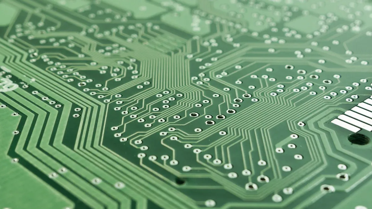
When you hear “definition pcb,” you learn about a key part in electronics. A printed circuit board, or PCB, is the main support for most electronic devices. You can find PCBs inside computers, phones, and toys. The definition pcb means a flat board that holds and connects parts. These boards use thin copper lines called traces to join parts. You can see these traces on top or inside the board.
A printed circuit board helps organize and hold electronic parts. You can think of a PCB as a map for electricity. The copper traces guide the current from one part to another. This careful layout is called pcb design. Good pcb design helps devices work safely and well. Most PCBs look green, but they can be other colors too. The green color comes from a layer called solder mask.
You use the definition pcb for both the board and how it connects parts. Without a printed circuit board, electronics would be messy and not work well. PCBs let us build small, strong devices that fit in your pocket.
PCB vs. PWB
You might also hear PWB, which means Printed Wiring Board. The definition pcb and PWB sound alike, but they are not the same. In the past, people used PWB for simple boards with only wiring paths. These boards did not have any parts on them yet. You could only see the copper lines on the board. As technology got better, people started using PCB more. Now, a printed circuit board means a board with wiring and parts on it.
The main difference between PCB and PWB is in their structure and use. PWBs are simple and often have one layer. They work for easy electronics that do not need many connections. PCBs can have many layers and support hard circuits. You find PCBs in advanced things like smartphones, computers, and medical tools. The definition pcb now means both the wiring and the parts that make the board work.
Note: In some places, like Japan, people still say PWB to avoid mix-ups with other meanings of PCB. In the United States, you usually see the word PCB.
Here is a table to help you see how PWB and PCB are different:
Aspect | PWB (Printed Wiring Board) | PCB (Printed Circuit Board) |
|---|---|---|
Definition | Gives paths for electrical connections only. | Gives paths and has electronic parts attached. |
Complexity | Usually simple, often one layer. | More complex; can be single, double-sided, or multilayer. |
Components | Does not come with parts already on it. | Comes with parts like resistors, capacitors, ICs, etc. |
Usage | Used in simple devices needing basic connections. | Used in hard devices needing many connections. |
Manufacturing | Simple process with basic etching and little drilling. | More complex process with advanced etching, drilling, and layers. |
Design | Focuses on paths on the board. | Needs careful layout for paths, parts, and vias. |
Thermal Management | Less worry because there are fewer parts and less heat. | Needs good heat control because of more heat. |
Cost | Usually cheaper because it is simple to make. | Costs more because it is harder to make. |
Applications | Good for easy things like power supplies and basic electronics. | Used in hard things like computers, smartphones, and medical tools. |
When you work with electronics, you use the definition pcb for the modern, complex boards in most devices today. You also use pcb design to plan how the traces and parts fit together. Knowing the difference between PCB and PWB helps you see how technology has changed over time.
Printed Circuit Board Structure
Layers and Materials
A printed circuit board looks flat and strong. But inside, it has many layers. These layers are stacked on top of each other. Each layer has a special job. The main pcb layers are substrate, copper, solder mask, and silkscreen. The substrate is the bottom layer. It makes the board strong. Most of the time, it is made from fiberglass and epoxy resin. This is called FR4. FR4 is strong and keeps electricity from leaking. Some boards use CEM-1 or CEM-3 for simple jobs. Flexible PCBs use polyimide. Polyimide bends easily and does not get damaged by heat.
There is a copper layer above the substrate. This layer lets electricity move around the board. The solder mask covers the copper. It keeps the copper safe from harm. It also stops solder from going where it should not. The silkscreen layer is on top. It adds words and symbols. These help you know where parts go. When you ask what pcbs are made of, you learn these layers work together.
Here is a table showing common components of printed circuit boards and their properties:
Layer/Material | Function | Key Properties |
|---|---|---|
Substrate (FR4) | Mechanical support | Strong, flame retardant, insulates well |
Copper | Electrical pathways | Conducts electricity, dissipates heat |
Solder Mask | Protection | Insulates, prevents short circuits |
Silkscreen | Identification | Adds readable labels |
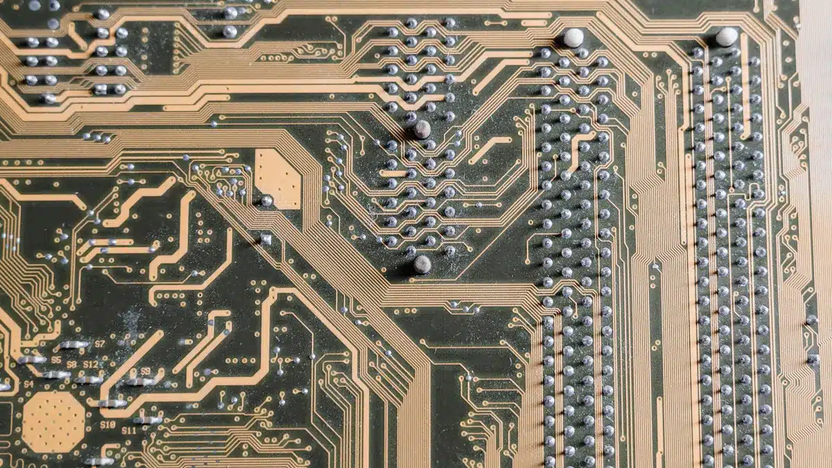
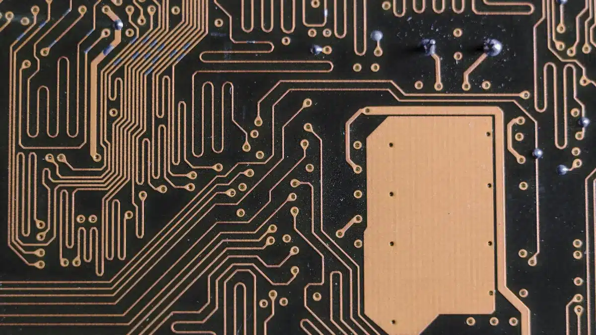
Copper Traces and Substrate
Copper traces are like roads for electricity. They are thin lines on the board. These lines connect parts like resistors and chips. Copper is used because it carries electricity well. It also helps with heat. If a trace is wide and thick, it can carry more power. This helps stop the board from getting too hot.
The substrate holds all the layers together. It keeps the board stiff or bendy, depending on what it is made of. FR4 is used for most boards because it is strong. Polyimide is used for flexible boards. You can bend these boards for things like wearables. Some boards use metal-core substrates like aluminum. These help get rid of heat in powerful devices.
When you look at pcb design, you see how layers and copper traces work as a team. Good design lets electricity move safely. It also keeps parts safe and in place. You must pick the right materials and trace sizes for your project.
Printed Circuit Boards Types
Printed circuit boards come in many shapes and sizes. There are different types of pcb for different jobs. Each type has special features. When you pick a board, you check how many layers it has. You also see if it bends or stays stiff. Let’s look at the main types of pcb you find in electronics.
Single-Sided, Double-Sided, Multilayer
There are three main types of pcb by layers:
Single-sided printed circuit boards have copper on one side only. These boards are for simple circuits. They cost less and are easy to make. You find them in calculators and LED lights. They are also in basic power supplies. These boards are good for low-density layouts.
Double-sided printed circuit boards have copper on both sides. Holes connect the two sides together. You get more space for parts. The signal paths are better too. These boards are in vending machines and car dashboards. They are also in phone systems. Use them when you need more connections but not too much complexity.
Multilayer printed circuit boards have three or more copper layers. Each layer has insulation between it. These boards are for advanced electronics. You can fit many parts in a small space. They are in smartphones and GPS devices. You also see them in medical equipment. These boards help reduce interference and boost performance.
Here is a table showing where each type is used:
PCB Type | Typical Applications |
|---|---|
Single-Sided PCB | Calculators, LED lighting, power supplies, cameras, printers |
Double-Sided PCB | Industrial controls, car dashboards, phone systems, vending machines |
Multilayer PCB | Smartphones, GPS systems, medical devices, aerospace, scientific equipment |
Tip: Pick the types of pcb that fit your needs for size, cost, and how hard the design is.
Flexible, Rigid, Rigid-Flex
You can also choose types of pcb by how they move:
Rigid printed circuit boards use strong fiberglass. These boards do not bend at all. You use them in computers and cars. They are also in industrial machines. They last a long time and cost less for big orders.
Flexible printed circuit boards use thin polyimide film. You can bend and twist these boards. They fit in wearable devices and medical implants. They are also in foldable phones. These boards save space and weight. But the design is harder and costs more.
Rigid-flex printed circuit boards mix stiff and bendy layers. You get the strength of rigid boards. You also get the flexibility of flex boards. These boards are in aerospace and military gear. They are also in advanced medical tools. They work well in tight spaces and tough places.
Here is a table to help you compare:
PCB Type | Structure Description | Typical Use Cases and Advantages |
|---|---|---|
Rigid PCB | Solid, inflexible substrate | Computers, cars, industrial equipment; strong and stable |
Flex PCB | Flexible polyimide film, bendable | Wearables, medical implants, foldable devices; saves space |
Rigid-Flex PCB | Mix of rigid and flexible layers | Aerospace, military, medical; compact and reliable |
Printed circuit boards come in many types. Each type helps you solve different problems in electronics. You pick the right board to make your electronic components work well and last longer.
PCB Function
Electrical Connections
A pcb helps make safe and steady electrical connections. The board works like a map for electricity. It guides power from one part to another. Many features help these connections happen:
The substrate holds the board together and keeps electricity in the right place.
Copper layers make thin lines called traces. These traces link all the parts.
Solder mask covers the copper. It stops the copper from rusting and keeps solder in the right spot.
Silkscreen puts words and symbols on the board. This helps you know where to put each part.
Vias are tiny holes with copper inside. They let electricity move between layers of the pcb.
Traces carry signals and power across the board.
Pads are small spots for soldering parts onto the pcb.
Ground and power planes are big copper areas. They spread out power and give a path for current to return.
You use soldering to attach parts to the pcb. Soldering connects the pins of parts to the pads. This makes a strong and safe connection. Sometimes, you use connectors or spring contacts. These help when you need to swap or move parts. All these ways make sure electricity moves safely and does not get lost.
Tip: Good connections help your devices last longer and stop problems like short circuits.
Mechanical Support
A pcb does more than just connect electricity. It also holds all the parts in place. The board is made of copper and special plastic layers pressed together. When you solder parts to the pads, they stay stuck to the board. This keeps everything safe, even if you shake or move the device.
Rigid pcbs use strong materials like FR-4. These boards do not bend. This keeps parts safe and stops them from breaking off. You can put the board inside a case and know the parts will not move. Flexible pcbs can bend and fit into small spaces or wearable gadgets.
The way a pcb holds and connects parts shows how it works in real life. You get both good electrical work and strong support in one board.
PCB Manufacturing
Design and Layout
You start the pcb manufacturing process with careful pcb design. This step shapes how your circuit board works and how reliable it will be. You use circuit board design software to draw the schematic. The schematic shows all the parts and how they connect. Next, you create the layout. You place each part on the board and draw the copper traces that link them. You must follow rules for trace width, spacing, and where to put holes. Good pcb design helps you avoid problems later.
Here are the main steps in pcb design and layout:
Draw the schematic to show parts and connections.
Import the schematic into a blank pcb layout.
Set up the stackup, which means choosing the number of layers.
Define design rules for trace width and spacing.
Place components on the board.
Route the traces to connect everything.
Check for errors with design rule checks.
Create files for manufacturing.
You can use many tools for pcb design. Popular choices include Altium Designer, KiCad, Autodesk EAGLE, and OrCAD. These tools help you with circuit board design, layout, and checking your work.
Fabrication Steps
After you finish the pcb design, you send the files to a factory. The factory uses these files to make your board. The process starts with printing your design onto films. The factory creates the substrate, which is the base of the board. They add copper layers and use light to harden the areas that will stay. Chemicals remove extra copper, leaving only the traces you designed. The factory stacks and presses the layers together. Machines drill holes for parts and connections. The board gets a solder mask and silkscreen labels. The last steps include cutting the board to shape and testing it for errors.
Quality control checks happen at every stage. These checks use machines like AOI and X-ray to find mistakes. Good quality control makes sure your pcb works well and lasts longer.
Assembly (PCBA)
When the blank board is ready, you move to pcb assembly. This step turns your board into a working device. First, machines put solder paste on the pads. Then, pick-and-place robots set each part in the right spot. The board goes through a reflow oven, which melts the solder and locks the parts in place. For some parts, you use through-hole soldering. After assembly, you test the board to make sure it works.
Printed circuit board assembly (PCBA) means your board now has all its parts and can do its job. PCBA is the final step before your device goes to market.
Blank PCB
A blank pcb is just the board with copper traces, holes, and labels. It has no parts attached yet. You use blank boards for testing, design, or as a base for printed circuit board assembly. Once you add the parts, the blank pcb becomes a PCBA. The blank board cannot work by itself, but it is the foundation for every electronic device.
Tip: Always check your circuit board design before sending it to the factory. Good pcb design saves time and money.
Printed circuit boards are very important in electronics today. They use copper traces and strong layers to connect parts. Protective layers help keep everything safe.
Single-sided boards are good for easy devices. Double-sided and multi-layer boards work for harder devices.
Flexible and rigid-flex boards let you make new shapes and smaller things.
PCBs help make strong and safe connections in devices. When you learn how these boards work, you get a useful skill for electronics.
FAQ
What does PCB stand for?
PCB stands for Printed Circuit Board. You see these boards in almost every electronic device. They connect and support electronic parts using copper traces.
Why do most PCBs look green?
Most boards look green because of the solder mask. This layer protects the copper traces and helps you see where to place parts. Manufacturers often choose green for better visibility during assembly.
Can you repair a damaged PCB?
You can repair some damaged boards if the damage is minor. You might fix broken traces with solder or special wire. Severe damage often means you need a replacement.
How do you clean a PCB safely?
You clean a board using isopropyl alcohol and a soft brush. This removes dust and leftover solder. Always turn off power before cleaning to avoid accidents.
What is the difference between a PCB and a breadboard?
A breadboard lets you build and test circuits without soldering. A PCB is a permanent board with fixed copper traces. You use breadboards for experiments and PCBs for finished products.
See Also
Understanding PCB Design And Its Importance In Electronics
Exploring PCBA Meaning And Its Function In Electronics
Defining PCBA In Electronics And Why It’s Essential