
The circuit board manufacturing process is crucial in electronics. Understanding each step is essential for you. It impacts both the quality and speed of production. By learning the entire circuit board manufacturing process—from design to testing—you can identify problems early. This knowledge simplifies work, reduces costs, and enhances product reliability. Implementing strict testing methods also ensures your printed circuit boards are of high quality, leading to more satisfied customers.
Key Takeaways
Begin with a clear drawing and layout design. This helps avoid expensive mistakes and makes sure parts fit well.
Pick the right materials like FR-4 for strength. Use copper for conductivity to make the board work better and last longer.
Follow exact steps like printing, etching, and drilling. This creates accurate and dependable circuit patterns.
Place parts carefully and use good soldering methods. This builds strong connections and lowers mistakes.
Test your boards well with visual and electrical checks. This finds problems early and improves product quality.
Design
Schematic Design
The schematic design is the first step to make a printed circuit board (PCB). In this phase, you turn your ideas into a picture. You make a diagram that shows how parts connect. A good schematic stops mistakes later on. Common design mistakes can cause big problems. For example, solder bridges can create shorts that harm parts. Tombstoning can make open circuits by pulling one side of a part away. You should always double-check your design files before sending them in to avoid these problems.
Layout Design
After finishing the schematic, you start layout design. This step is about placing the parts on the PCB. You need to think about things like trace width and spacing. Good trace design stops electrical failures and signal problems. Special software tools can help you with this job. Here are some popular choices:
Altium Designer – Known for being easy to use and having great features.
Eagle – Simple and liked by hobbyists.
KiCad – A free tool that is becoming popular for custom designs.
OrCAD – Has simulation and analysis tools for experts.
Using these tools can make your design work easier and more accurate. They help you see the board and make sure all parts fit well.
Materials
In the PCB manufacturing process, picking the right materials is very important. You must know the types of materials used. They affect how well your printed circuit board works and how reliable it is.
Substrate Materials
Substrates are the base for your PCB. They give support and keep electricity from leaking. Here are some common substrate materials:
FR-4: This is the most popular substrate. It has good strength and insulation at a low price. You can use it for many applications.
Flexible substrates: Made from materials like polyimide, these can bend and fit into small spaces. They are great for wearables and medical devices.
Metal core substrates: These help manage heat better. They are good for high-power uses like LED lighting.
Ceramic substrates: Known for their great heat conductivity, they work well in high-frequency and power circuits.
Specialized materials: Options like Rogers and Teflon-based substrates are made for low signal loss. They keep signals strong in RF and microwave uses.
Here’s a quick comparison of some substrate materials:
Substrate Material Type | Description and Advantages | Typical Applications |
|---|---|---|
FR-4 | Low cost, good strength | Consumer electronics |
Flexible Materials | Can bend, high heat resistance | Wearables, medical devices |
Metal Core Substrates | Better heat management | LED lighting, power electronics |
Ceramic Substrates | Great heat conductivity | High-frequency circuits |
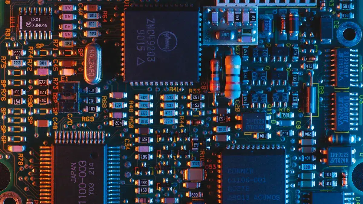
Conductive Materials
Conductive materials are also very important. They affect how well your printed circuit board works. The most common conductive material is copper. It has great electrical conductivity, making it cheap and reliable for many uses.
Other materials include:
Silver and Gold: These are used in special cases for their great conductivity and resistance to rust. They are best for high-frequency circuits.
Ceramic substrates: They have high heat conductivity and stability, good for high-power uses.
Insulated Metal Substrates (IMS): These help with heat loss, making them more reliable in high-power electronics.
Here’s a table showing how different conductive materials affect performance:
Conductive Material | Influence on Performance | Typical Applications | Advantages |
|---|---|---|---|
Copper | Great conductivity | General PCBs | Affordable |
Silver and Gold | Great conductivity | High-frequency PCBs | Rust resistance |
Ceramic Substrates | High heat conductivity | Power electronics | Great heat loss management |
Choosing the right materials helps your printed circuit board work well and last longer.
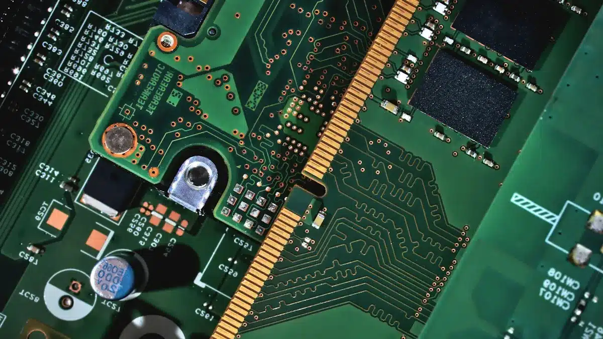
Fabrication Steps
The fabrication steps are very important in making printed circuit boards (PCBs). Each step helps decide how good and useful the final product will be. Let’s look at the main fabrication steps:
Printing Layers
The first step in making a PCB is printing the layers. You put a photoresist material on the substrate. This special material reacts to light and protects certain areas during etching. It makes sure that only the right circuit patterns stay after etching. This accuracy affects how well the board works and its production costs.
However, problems can happen during this step. For example, missing or wrong Gerber files can cause design mistakes. Leaving out parts in the Bill of Materials (BOM) can slow down assembly. Also, not thinking about things like temperature and moisture can lead to warping or rust.
Here are some common problems you might face during the printing layer process:
Challenge Category | Description | Consequences / Effects |
|---|---|---|
Design Errors | Mistakes like wrong component placement and bad trace routing. | Delays, malfunction, signal problems. |
Material Selection | Picking the wrong materials that affect strength and heat management. | Less reliability, heat issues, higher costs. |
Manufacturing Defects | Surface problems and poor copper plating. | Open connections, solder bridges, shorts. |
Etching Process
Next, you go to the etching process. This step removes unwanted copper to show the circuit patterns. You start by putting a photoresist layer on to protect areas that should stay copper. After developing the photoresist, you expose the PCB to an etchant that dissolves the extra copper. This careful process allows for exact removal of copper, which affects how accurate and strong the final PCB circuits are.
How precise the etching is depends on things like etchant strength and temperature control. Keeping the right temperature, usually between 45–55°C, is very important. It affects how fast and evenly the copper is removed. Quality checks, like automated optical inspection (AOI), help find problems early, making sure the circuits are good.
Drilling and Plating
The last step in the fabrication process is drilling and plating. Computer-controlled drilling makes holes for connections between layers. This step needs to be very precise to keep everything connected. After drilling, you coat the holes with a conductive material through a process called via plating. This keeps signals strong and reliable.
Each of these fabrication steps is very important in the PCB manufacturing process. They make sure your printed circuit boards meet the needed standards and work properly. By focusing on precision and quality checks, you can reduce problems and improve the reliability of your final product.
Assembly
The assembly process is an important part of making PCBs. It includes putting components on the printed circuit boards and making sure they are connected well. Good assembly affects how well the final product works and how reliable it is.
Component Placement
You need to plan where to put components on the PCB carefully. Here are some good ways to improve component placement:
Group components by their main functions. Keep high-speed digital, analog, and power parts apart to reduce noise.
Keep digital and analog grounds separate. This helps reduce interference.
Spread out heat-generating components. Use thermal vias and heat sinks to prevent hot spots.
Align all IC pin 1 markers in the same direction. This makes assembly easier and cuts down on mistakes.
Place smaller components before larger ones. This prevents blocking during wave soldering.
Put board-to-wire connectors near the edges. This keeps things organized and avoids unwanted contact.
Make sure there is enough space for copper traces, especially near high-pin-count components. This helps with routing.
Following these tips helps you create a well-organized PCB layout, which is key for a successful PCB assembly process.
Soldering Techniques
Soldering is how you connect components to the PCB. Different soldering methods can greatly affect how reliable and long-lasting your assembled circuit boards are. Here are some common techniques:
Surface Mount Technology (SMT): This method allows for smaller designs and better resistance to vibrations. It improves high-frequency performance, which can make devices last longer.
Through-Hole Technology (THT): This technique gives stronger connections. It works well for high-power components and applications needing strong physical links.
Reflow Soldering: This automated method improves the quality of solder joints, helping the PCB last longer.
Wave Soldering: This method is often used for THT components and ensures strong connections.
Choosing the right soldering method is very important. It affects how strong the connections are and how well heat is managed, both of which are key for the long-term reliability of your printed circuit boards.
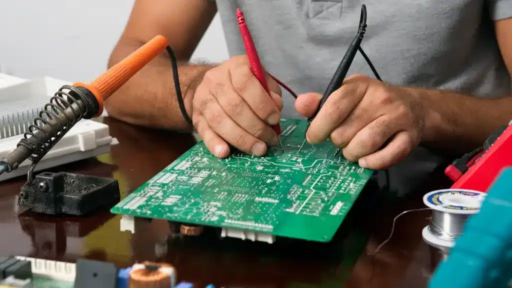
Testing
Testing is very important in making circuit boards. It makes sure your printed circuit boards (PCBs) work well and meet quality standards. By using strong testing methods, you can find problems early. This helps avoid expensive recalls and makes customers happier. Here are some main reasons why testing is important:
Testing finds problems early, reducing waste and extra costs.
It checks if the design matches, including electrical and size accuracy.
Testing stops expensive failures in the field, protecting your company’s name.
It raises product quality and customer happiness.
Testing keeps control of the process by giving data to improve manufacturing.
Visual Inspection
Visual inspection is one of the easiest and best ways to find defects. You can do this by hand or use machines like Automated Optical Inspection (AOI). During visual inspection, you look for clear defects like solder bridges, misaligned parts, and other surface problems. This method helps catch issues early, saving time and resources later in production.
Tip: Always use visual inspection with automated methods to make it more accurate and efficient.
Electrical Testing
Electrical testing checks that your PCB meets its design goals. This process includes different methods, each with a specific purpose:
Testing Method | Objective | Why It Is Needed |
|---|---|---|
In-circuit testing using spring-loaded pins to check connections and part functions. | Fast, simultaneous testing for mass production; finds open/short circuits and assembly issues. | |
Automatic Optical Inspection (AOI) | Visual inspection using cameras and image processing to find soldering and part defects. | Automates inspection; quicker and more accurate than manual; cuts down on rework and field failures. |
Checks if PCB does its intended jobs under set conditions. | Confirms overall device function; final check before shipping. | |
Flying Probe Testing | In-circuit testing with movable probes, no special fixture needed. | Flexible for prototypes and small batches; finds open circuits and wrong parts. |
These methods help find faults early, saving you time and money. By adding automated testing systems, you can get consistent, repeatable, and fair results. This reduces human mistakes and improves test coverage, leading to better yield rates in your PCB production.
In short, the PCB manufacturing process has important steps. These steps help make sure your final product works well. Each part is very important:
Design: Good design reduces mistakes and helps with making.
Materials: Picking the right materials affects how well it works and lasts.
Fabrication: Careful steps like etching and drilling keep the electrical parts working.
Assembly: Good placement of parts and soldering makes strong connections.
Testing: Strong testing methods find problems early, saving money and improving reliability.
By following these steps, you can create high-quality PCBs that meet industry standards and please customers. Remember, paying attention to details at every step leads to better performance and longer life for your electronic devices. 🌟
FAQ
What is a PCB?
A PCB, or printed circuit board, is a board that connects electronic parts. It gives support and electrical links using conductive paths. You can find PCBs in nearly all electronic devices.
Why is testing important in PCB manufacturing?
Testing makes sure your PCBs work right and meet quality standards. It helps you find problems early, which cuts down waste and costs. Good testing boosts reliability and makes customers happy.
What materials are commonly used in PCBs?
Common materials are FR-4 for substrates and copper for conductive paths. You might also see flexible materials for bendable designs and metal cores for better heat control.
How does the assembly process work?
The assembly process includes putting parts on the PCB and connecting them with soldering. Good placement and soldering methods make strong connections and reliable performance.
What software can I use for PCB design?
You can use software like Altium Designer, Eagle, KiCad, and OrCAD for PCB design. These tools help you make accurate schematics and layouts, making the design process easier and faster.
See Also
An In-Depth Overview Of PCBA Manufacturing Procedures
Detailed Stepwise Instructions For PCBA Production Workflow
Key Phases In The PCBA Assembly And Production
Essential Advice For Overcoming PCBA Production Difficulties