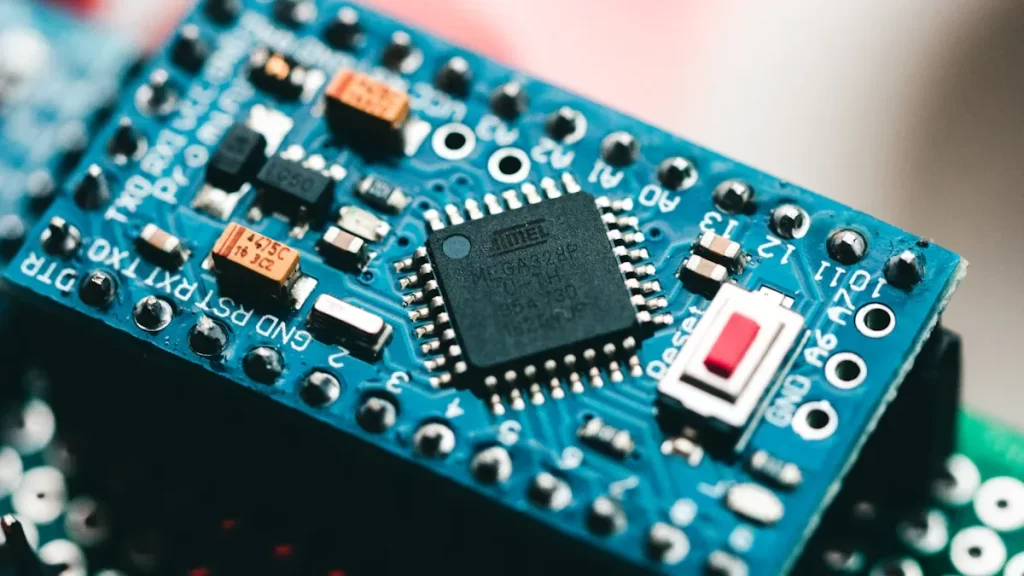

Compact PCB for edge sensors are small yet highly functional boards designed to integrate seamlessly with advanced sensor technology. These compact PCB for edge sensors enable sensors to process data locally, enhancing speed and reducing latency for quicker decision-making. Their miniature size makes them ideal for devices such as IoT gadgets, smartwatches, and smart home tools.
The significance of compact PCB for edge sensors is evident in modern technology trends. For example, the rapid expansion of IoT demands PCBs that efficiently connect sensors. Innovative packaging techniques, such as System-in-Package (SiP), merge multiple components into a single unit, optimizing space and performance. As technology continues to evolve, compact PCB for edge sensors remain crucial across various applications and industries.
Key Takeaways
Small PCBs help edge sensors process data nearby. This makes decisions faster and lowers delays.
Tiny PCBs are important for new tech. They make things like smartwatches and IoT devices smaller, lighter, and better.
Using methods like Surface Mount Technology (SMT) saves space and energy. This helps devices last longer on battery.
Small PCBs are built to handle tough conditions. They work well in cars and factory machines.
These PCBs are key in many fields like healthcare, farming, and environment tracking. They help collect and process data easily.
Understanding Compact PCBs for Edge Sensors
What Are Compact PCBs for Edge Sensors?
Compact PCBs for edge sensors are tiny circuit boards. They are made to work with advanced sensor systems. These boards are small but very powerful. They let sensors handle data nearby instead of using big systems. Their small size helps them fit into tight spaces. Devices like smartwatches, IoT tools, and factory machines use them.
These PCBs are built with surface mount technology (SMT). SMT places parts directly on the board’s surface. This makes the PCB smaller but still very useful. For example, the InSeKT project uses compact PCBs to add AI to edge sensors. This makes data processing faster and safer. It also allows real-time actions while keeping the sensors small.
How They Enhance Edge Sensor Functionality
Compact PCBs make edge sensors work better. They let sensors process data nearby, which speeds up decisions. This is very important for things like self-driving cars and factory robots. These need quick reactions to work well.
Using SMT makes these PCBs even better. SMT lets more parts fit on smaller boards. For example, the AI-Vision Edge Box camera uses a six-layer PCB with SMT. It processes data in just 6 milliseconds, showing how compact PCBs improve sensors.
Compact PCBs also reduce electrical noise, making signals clearer. Techniques like via-in-pad routing help parts communicate better. These features make compact PCBs a must-have for high-tech sensors.
The Role of Miniaturization in Modern Applications
Making PCBs smaller is key to their success. Tiny boards make devices lighter, faster, and more useful. You can see this in healthcare and space exploration. For example, small PCBs are used in glucose monitors. These devices need to work well in a tiny size.
New ways to make PCBs smaller have improved them even more. Advanced SMT and via-in-pad methods save space and manage heat better. In satellites, smaller PCBs lower launch costs. They also let more satellites launch together, making space missions cheaper and effective.
Miniaturization also helps in farming and environmental monitoring. Tools like soil sensors use small PCBs and energy harvesters. These devices work for a long time without batteries. They send important data from far away, showing how useful small PCBs are today.
Features and Benefits of Compact PCBs for Edge Sensors
Space Efficiency and Miniaturization
Compact PCBs save space but still work really well. They use Surface Mount Technology (SMT) to put parts directly on the board. This makes the board smaller and fits more parts in less space. Devices like smartphones and IoT gadgets use these boards to stay small and light.
Engineers plan the layout carefully to save space. They group parts by what they do and keep wires short. Removing extra parts also helps make the board smaller. These steps make sure compact PCBs meet size, weight, and power (SWaP) needs for modern devices.
Power Efficiency and Extended Battery Life
Compact PCBs are small and use less energy. Their design helps save power, which is great for battery-run devices like wearables. SMT keeps parts close together, cutting energy loss and boosting performance.
Smaller PCBs also make devices need less power to work. This helps batteries last longer, which is important for tools like environmental sensors. These sensors often have limited power. Compact PCBs make sure devices work well and last a long time.
Signal Integrity and Reduced Electrical Noise
Compact PCBs keep signals clear and strong. They lower electrical noise using tricks like via-in-pad routing. This helps parts talk to each other better, which is key for things like medical tools and self-driving cars.
Having parts close together also stops signal problems. Shorter paths for electricity improve how well the board works. Compact PCBs are great for high-tech tools in healthcare and factories. They give steady and reliable results every time.
Durability and Reliability in Harsh Environments
Compact PCBs for edge sensors are built to handle tough conditions. They work well even in extreme environments. Their strong design and careful testing make this possible.
Manufacturers test compact PCBs with thermal cycling. This checks how they handle big temperature changes. These tests mimic harsh conditions to find weak spots. For example, quick temperature shifts ensure the materials and parts won’t fail.
Did you know? Shock and vibration tests are also important. These tests copy real-life situations like car vibrations or machine impacts. They make sure the PCB can survive tough challenges.
Here’s a simple table of common tests:
Testing Methodology | What It Checks |
|---|---|
Tests if vehicles handle heat and rough roads. | |
Shock and Vibration Testing | Checks if PCBs survive shakes and impacts. |
To make them tougher, compact PCBs use precise temperature controls. Custom tests are made for different uses. For example, in factories, PCBs face dust, moisture, and shaking but still work well.
By focusing on strength and dependability, compact PCBs keep devices running smoothly. Whether in cars, wearables, or sensors, these boards are key to modern technology.
Applications of Compact PCBs for Edge Sensors

IoT Devices and Smart Home Systems
Compact PCBs are important for IoT and smart home gadgets. These small boards connect sensors, processors, and communication parts. They help devices work well in tight spaces. You can find them in things like thermostats, smart lights, and security cameras. Their tiny size and strong performance make them perfect for smart homes.
For instance, smart locks use compact PCBs for smooth operation and strong connections. These boards allow real-time data sharing, improving user experience. Similarly, smart lights use PCBs to adjust brightness based on room light. This saves energy and makes life easier.
Here’s a simple table of their uses:
Application Case Study | Description |
|---|---|
Smart Home Devices | PCBs help connect devices like thermostats and smart locks. |
Smart Home Gadgets | Gadgets like lights and cameras use PCBs for sensors and processors. |
Compact PCBs let IoT devices do more without using extra space or power. This makes them essential for today’s smart homes.
Healthcare and Wearable Technology
Compact PCBs are changing healthcare tools and wearable gadgets. Their small size allows for portable devices with advanced features. You’ll see them in glucose monitors, heart trackers, and health wearables. These devices give useful health data while staying comfy and reliable.
Flexible PCBs are key for wearables. They bend to fit clothes or skin, making them easy to wear. For example, rigid-flex PCBs mix stiff and bendy parts. This makes them great for wearables needing both strength and flexibility. These designs are boosting demand for lightweight medical gadgets.
Here’s a quick look at healthcare trends:
Trend | Description |
|---|---|
Smaller devices with advanced features in tiny spaces. | |
Flexible and Stretchable PCBs | PCBs that fit clothes or skin for comfy wearables. |
Interconnected Systems | IoT links for easy data sharing and remote health checks. |
Energy Harvesting | PCBs designed to save energy for medical tools. |
Compact PCBs also help with constant health tracking in IoMT devices. They ensure accurate data in small designs, making them vital for wearables and medical tools.
Automotive Systems and Autonomous Vehicles
Compact PCBs are improving cars and self-driving vehicles. Modern cars have over 200 control units, many using compact PCBs. These boards handle complex circuits while staying strong under stress.
Multi-layer PCBs are very important for self-driving cars. They process data fast, helping with quick decisions. For example, HDI PCBs manage tricky circuits in small spaces. They work reliably in autonomous systems. Their light weight also helps cars use less fuel.
Key points about their role in cars:
Multi-layer PCBs boost performance in advanced car systems.
Compact designs shrink control units, making cars more efficient.
The self-driving car market may hit $556 billion by 2035, showing the need for better PCBs.
Lightweight PCBs help save fuel and lower environmental harm.
Compact PCBs make sure car sensors work well, even in tough conditions. Their ability to handle hard tasks in small spaces makes them crucial for future cars.
Industrial Automation and Robotics
Compact PCBs are crucial for industrial automation and robotics. They help machines work better by combining sensors, processors, and communication parts into small, strong boards. These boards let robots and systems handle data fast and make accurate decisions instantly. This is important for industries wanting to boost production and cut costs.
In factories, compact PCBs save space inside machines. For example, robotic arms on assembly lines use these boards to move precisely. Their tiny size helps make smaller robots that fit in tight spots. This increases efficiency without needing extra room.
Here are some real-world examples of compact PCBs in action:
Eutron Kunshan solved space and efficiency issues with PCB-powered automation.
Amer SpA improved material handling by fully automating its processes.
Elektramat met high order demands using PCB-based automation systems.
Compact PCBs offer more than just space-saving benefits. They also increase production, lower defect rates, and use less energy. For instance, a smartphone company raised production from 10,000 to 85,000 units daily while cutting defects from 2% to 0.02%. Similarly, an automotive supplier improved product quality from 92% to 99.7%, reducing warranty claims by 83%.
Case Study | Production Capacity | Defect Rate | Labor Cost Reduction | Time-to-Market Reduction | Energy Consumption Reduction |
|---|---|---|---|---|---|
Smartphone Manufacturer | 10,000 to 85,000 units/day | 2% to 0.02% | 78% per unit | 65% | 42% |
Automotive Supplier | 230+ product variants | 92% to 99.7% | N/A | N/A | N/A |
Medical Implant Manufacturer | 100 to 5,000 units/month | N/A | N/A | 61% | N/A |
Compact PCBs also make industrial robots tougher. They can handle extreme heat, vibrations, and dust. This durability keeps machines running smoothly, making them essential for industrial use.
Environmental Monitoring and Smart Agriculture
Compact PCBs are changing environmental monitoring and smart farming. They help create small, energy-saving devices that collect and process data in faraway places. These tools check soil, weather, and air quality, giving useful information for eco-friendly practices.
In smart farming, compact PCBs power sensors that measure soil moisture, temperature, and nutrients. These sensors help farmers use water and fertilizers wisely, saving resources. For example, soil sensors with compact PCBs send live data to IoT devices. This helps farmers make better choices for crops.
Environmental monitoring also uses compact PCBs. Devices like air quality monitors and weather stations depend on these boards to process data and send it to IoT systems. Their small size and low energy use make them perfect for remote areas.
Another benefit is energy harvesting. Many sensors use solar panels or other renewable energy sources. This means they can work for a long time without needing new batteries, saving money and helping the environment.
Compact PCBs also improve precision farming. They work with IoT devices to guide drones and robotic harvesters. These systems perform tasks accurately, boosting productivity and sustainability. This helps meet the growing need for efficient food production.
Tip: Compact PCBs in farming and environmental tools save energy and support green practices. Their ability to work in remote areas with little power makes them a big step forward for sustainability.
Challenges in Compact PCB Design and Manufacturing
Heat Dissipation in Small Form Factors
Handling heat in small PCBs is a big challenge. Smaller boards have less space to release heat. This increases power and can cause overheating. Good heat management is needed for reliable performance. Techniques like better layouts, thermal vias, and special materials help spread heat. For example, SMD heat sinks are often used to control heat in tight spaces. These methods keep parts cooler and make them last longer.
Evidence Type | Description |
|---|---|
SMD Heat Sinks | Important tools for controlling heat in small PCBs. |
Thermal Management Strategies | Methods like better layouts and cooling technologies. |
Challenges of Miniaturization | Less space for heat release and higher power density. |
Component Reliability | Cooler parts last longer and work better. |
PCB Design Optimization | Using thermal vias improves heat control. |
Tip: Managing heat well helps your PCB work better and last longer.
Ensuring Signal Integrity and Performance
Keeping signals clear in small PCBs needs careful design. Fast signals can face problems like bad routing or poor grounding. These issues can distort signals and lower performance. Engineers use tricks like via design and ground planes to fix this. Keeping enough space between signal paths also avoids interference. Solving these problems ensures parts communicate properly.
A good signal design means knowing how choices affect performance. For example, bad grounding can cause noise, and poor routing can lose signals. Engineers must focus on these fixes to make reliable small PCBs.
Material and Component Selection Constraints
Picking the right materials for small PCBs is tricky. It’s a balance between cost, performance, and making them. Rigid PCBs are cheaper but not flexible. Flexible PCBs bend easily but cost more. Hybrid designs save space and improve reliability but need big investments.
PCB Type | Cost Factors | Benefits | Limitations |
|---|---|---|---|
Cheaper materials and simpler to make. | Well-known tech, low cost. | Not flexible, needs extra connectors. | |
Pure Flexible PCBs | Higher material and making costs. | Very flexible, fewer connectors needed. | Expensive materials and special processes. |
Newer Technological Alternatives | High initial costs for materials and making. | Smaller size, better reliability. | Expensive to start, limited material options. |
Note: The materials you choose affect cost and how well the PCB works. Balancing these is key for smart designs.
Balancing Cost and Production Efficiency
Making compact PCBs for edge sensors needs smart cost and efficiency planning. This balance keeps your product affordable, reliable, and high-performing. But, it comes with challenges that need careful thought and decisions.
To save money, improve the PCB design. Use layouts that waste less material and shrink unused spaces. Picking standard board sizes and parts also cuts costs. For example, using ready-made parts instead of custom ones saves money without losing quality.
Another way to save is by improving production. Automated machines make work faster and cheaper. Partnering with experts in compact PCBs ensures good quality and efficient production.
Tip: Talk to your PCB maker early in the design process. This helps find ways to save money and avoid costly changes later.
Choosing the right materials is also important. Good materials may cost more upfront but save money over time. They last longer and work better. For instance, materials that spread heat well can lower cooling needs, saving energy and extending PCB life.
Here’s a simple table of cost-saving ideas:
Strategy | Benefit | Example |
|---|---|---|
Better PCB Design | Uses less material | Smaller boards |
Standard Parts | Cuts production costs | Ready-made resistors |
Automated Production | Speeds up work | Robotic assembly |
Quality Materials | Lasts longer, works better | Heat-spreading materials |
By using these ideas, you can make compact PCBs that are affordable and efficient. This way, your designs meet industry needs without going over budget.
Solutions to Overcome Challenges in Compact PCB Design
Using Advanced Design Tools
Advanced tools help fix compact PCB design problems. These tools find and solve issues before making the PCB. For example, impedance control keeps signals clear by managing trace paths. Signal termination stops reflections, improving how signals work. Tools like SPICE and 3D solvers help check and improve designs for better results.
Here’s a table of helpful techniques and tools:
Technique/Tool | What It Does |
|---|---|
Impedance Control | Keeps signals clear by managing trace paths. |
Signal Termination | Stops reflections and improves signal quality. |
Signal Analysis Tools | Matches trace paths and reduces signal problems. |
SPICE | Checks signal quality and finds interference issues. |
Electromagnetic Simulators | Models signal problems with high accuracy. |
3D Field Solvers | Gives detailed checks for signal issues in circuits. |
Using these tools ensures your PCB works well and stays reliable.
Picking Good Materials and Parts
High-quality materials make PCBs last longer and work better. Materials with good heat and electrical properties improve performance. Testing methods like optical and X-ray checks ensure all parts meet standards.
Common PCB tests include:
In-Circuit Testing (ICT)
Flying Probe Test
Functional Test
Automated Optical Inspection (AOI)
X-Ray Inspection
Electrical Testing
Following rules like IPC-A-610 and ISO 9001 ensures consistent quality. These steps help create PCBs that work well in tough conditions.
Teaming Up with PCB Experts
Working with skilled PCB makers makes designing easier. Experts help pick materials, improve layouts, and save costs. They also use advanced methods to make high-quality PCBs.
Starting early with experts helps find and fix problems quickly. Experienced manufacturers ensure your PCB works well and stays affordable. This teamwork helps meet both technical and budget needs.
Rigorous Testing and Quality Assurance
Testing makes sure a PCB works well and is reliable. Using strong testing methods helps find problems early. This saves time and money during production.
One important test is functional testing. It checks if the PCB works as it should in normal conditions. For example, you can create real-life situations to see if the board processes data correctly. Another key test is thermal testing. It looks at how the PCB handles heat, which is crucial for small designs that can overheat.
Environmental testing is also very important. It ensures the PCB stays reliable in tough conditions like heat, shaking, or moisture. For instance, vibration tests copy the shaking that happens in cars or factories. These tests make sure the PCB stays strong and works properly.
Automated Optical Inspection (AOI) is another useful tool. Cameras check for problems like misplaced parts or bad soldering. This method is fast and accurate. X-ray testing can also find hidden issues, like cracks or gaps in solder joints.
By using these tests, you can make sure your PCBs are reliable and perform well. Testing improves quality and builds trust with users.
Tip: Keep records of your test results. This helps track progress and meet industry rules.
Compact PCBs for edge sensors are very important in today’s tech. They help devices work faster, use less power, and fit in tight spaces. Their strong build and clear signals make them useful in fields like healthcare, cars, and farming.
In the future, compact PCBs will keep improving IoT and edge computing. As tech grows, these small but powerful boards will create new ideas, making gadgets smarter and better.
FAQ
What are compact PCBs, and why are they important for edge sensors?
Compact PCBs are tiny circuit boards made for small spaces. They help edge sensors process data nearby, making them faster. Their small size and efficiency are perfect for modern devices like IoT tools, wearables, and smart systems.
How do compact PCBs improve battery life in devices?
Compact PCBs are designed to save energy and use less power. By keeping parts close together, they waste less energy. This helps batteries last longer in devices like smartwatches, medical tools, and environmental sensors.
Can compact PCBs handle extreme environments?
Yes, compact PCBs are made to work in tough conditions. They are tested for heat, shaking, and moisture to ensure they are strong. These tests make them reliable for use in factories, cars, and outdoor sensors.
What industries benefit the most from compact PCBs?
Industries like healthcare, cars, farming, and IoT gain a lot. Compact PCBs make wearable health devices, self-driving cars, smart farm tools, and connected home gadgets work well in small spaces.
How do compact PCBs support IoT devices?
Compact PCBs combine sensors, processors, and communication parts on one board. This helps IoT devices collect, process, and share data easily. Their small size and efficiency make them great for smart home and industrial IoT tools.
See Also
Exploring PCBA Meaning and Its Essential Uses in Electronics
The Advantages and Uses of PCBA in Today’s Electronics
Navigating PCBA Applications in Consumer Electronics Today