
PCBA failure analysis means finding out why circuit boards fail. This step is very important in making good and reliable electronics. By studying failures, weak spots in design or making can be found. Fixing these can make big improvements. For example, studies show failure rates drop by 57% with good analysis. Solving problems early saves money, avoids delays, and meets quality rules like IPC-A-610. This method helps create stronger and more reliable PCBs while improving how they are made.
Key Takeaways
PCBA failure analysis finds out why circuit boards stop working. This helps make them more reliable and better performing.
Tools like Automated Optical Inspection (AOI) and X-rays spot problems early. This saves both time and money.
Following clear steps helps find and fix problems completely. This makes the product work better overall.
Using plans like Design for Reliability (DFR) prevents future issues. It also makes the manufacturing process better.
Writing down details of problems and solutions helps improve products. It also ensures they meet industry rules.
Understanding PCBA Failure Analysis
Definition and Objectives
PCBA failure analysis means finding out why circuit boards fail. It helps discover problems and make PCBs more reliable. By studying failures, you can improve how PCBs are made. This also ensures they meet quality rules like IPC-A-610. The main goals are to fix defects, boost performance, and save money on repairs.
It also focuses on the most serious problems first. For example, spotting bad soldering or broken parts early avoids bigger issues later. This step-by-step method ensures PCBs work well and handle tough conditions.
Key Tools and Techniques
To study PCBA failures, you need special tools and methods. Automated Optical Inspection (AOI) and X-rays find soldering mistakes or hidden damage. Tests like heating and moisture checks show how PCBs handle tough environments.
New methods, like AI tools, make finding problems easier. Over half of PCB checks now use AI for better results. Careful studies, like checking copper connections, have solved making issues and improved cleaning steps.
Importance of a Systematic Approach
A clear plan is key for good PCBA failure analysis. It makes sure every step, like finding and fixing problems, is done right. Keeping records of issues helps trace problems back to their cause. This improves designs and makes the supply chain better.
By following a clear plan, you can find problems early and stop them. This makes PCBs more reliable and saves time and money.
Common Failure Modes in PCBA
Electrical Failures
Electrical problems happen often in circuit boards. These issues occur when electricity cannot flow correctly. Causes include unstable voltage, weak signals, and short circuits. For instance, a broken capacitor or resistor can stop current flow. Bad soldering, like cold joints, also leads to these problems.
To find electrical issues, tools like AOI and X-rays are useful. They detect problems like misplaced parts or broken connections. Tests, such as checking continuity and function, ensure the board works. Fixing these problems early makes boards more reliable.
Mechanical Failures
Mechanical problems come from physical stress on the board. Vibrations, shocks, and bad soldering often cause these issues. They can loosen parts, crack solder, or break traces. About 20% of PCB failures are mechanical, making them important to address.
To avoid these issues, use strong soldering methods and good materials. Tests like vibration and shock simulations check how boards handle stress. Keeping records of problems helps improve future designs.
Thermal Failures
Thermal problems happen when boards get too hot. Heat can harm parts, weaken solder, and cause failure. High-power boards are more at risk. Poor heat management, like bad heat sinks, makes it worse.
Thermal cycling tests and heat-resistant materials can fix this. Better designs, like adding thermal vias, help remove heat. Managing heat well lowers failure risks and makes boards last longer.
Environmental Failures
Outside conditions can harm how PCBAs work and last. These failures happen when things like water, heat changes, or dirt damage the board. Knowing these dangers helps make stronger and better electronics.
Common Environmental Stressors
Different outside factors can cause PCBA problems:
Humidity and Moisture: Water can get inside and cause rust or shorts. This often happens in wet or outdoor places.
Temperature Extremes: Big temperature changes can crack solder or break parts.
Contaminants: Dust, dirt, and chemicals can mess up connections.
UV Exposure: Sunlight over time can weaken materials, especially outdoors.
Tip: Use special coatings to protect PCBAs from water, dust, and dirt.
Testing for Environmental Failures
You can test PCBAs by copying tough conditions. These tests include:
Thermal Cycling: Heating and cooling the board many times to find cracks.
Humidity Testing: Putting the board in wet air to check for rust.
Salt Spray Testing: Using salty air to see if the board resists rust, good for sea use.
Preventive Measures
To stop these problems, you can:
Pick materials that don’t rust or get damaged by sunlight.
Add coatings to keep water and dirt away from the board.
Make cases that block harsh weather from reaching the board.
By fixing these risks early, PCBAs can work better and last longer.
Step-by-Step Methods for Conducting PCBA Failure Analysis
Problem Definition and Data Collection
The first step is to clearly define the problem. Gather all important details about the PCBA failure. This includes knowing the symptoms and when it happened. Check where the failure occurred and what conditions caused it. For example, was the board in high heat or wet places? Did it fail during testing, assembly, or use?
Start by collecting records like production logs and test results. Customer feedback can also help find the issue. Write down the type of failure, like electrical, mechanical, or thermal. Use a system to rank problems by how serious they are. Focus on the most critical issues first. This way, you can find and fix the main cause quickly.
Tip: Make a list of possible causes like bad soldering or old parts. This keeps you organized and ensures nothing is missed.
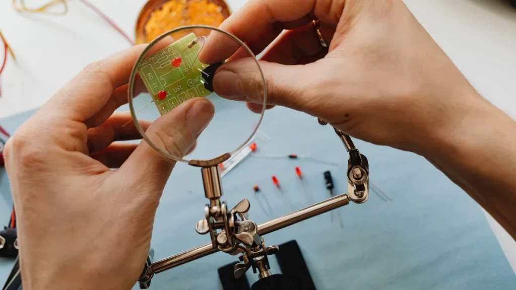
Visual Inspection and Non-Destructive Testing
After defining the problem, check the PCBA for visible damage. Look for cracked solder, burnt parts, or misaligned components. Use tools like magnifying glasses or microscopes to see small defects.
Non-destructive testing is very helpful here. Tools like Automated Optical Inspection (AOI) and X-rays find hidden problems without harming the board. AOI is great for spotting soldering mistakes. X-rays can show internal issues like gaps in solder or misaligned layers. These methods save time and keep the board safe for more tests.
Note: Non-destructive testing finds faults and checks if the board was made correctly. It ensures the board meets standards like IPC-A-610.
Electrical Testing and Functional Analysis
Next, test the board’s electrical performance. Electrical tests find problems like unstable voltage or short circuits. Start with continuity tests to check if connections work. Then, do functional tests to see if the board works as it should.
For harder problems, use tools like oscilloscopes or multimeters. These tools measure electrical signals and find faulty parts like broken resistors. Functional analysis also tests the board in real-world conditions. This helps find hidden problems that normal tests might miss.
By using these methods, you can find the main cause of the failure. Then, you can suggest fixes. For example, if overheating caused the problem, you might add heat sinks or thermal vias to the design.
Destructive Testing and Material Analysis
Destructive testing is used when non-destructive methods fail. It involves breaking the PCB to study its inside parts. This helps find hidden problems that surface checks might miss.
Common Destructive Testing Methods
Cross-Sectional Analysis: Cut the PCB to see its inside layers. This finds problems like cracks, gaps, or bad solder joints.
Thermal Stress Testing: Heat or cool the PCB to test its strength. This shows weak spots in solder or materials under real-world conditions.
Chemical Analysis: Remove layers of the PCB to study its materials. This helps find dirt or low-quality materials.
Shear Testing: Push on parts or solder joints to test their strength. Weak parts break, showing design or making problems.
Tip: Write down all results from destructive tests. This keeps a record of the problem and helps improve future designs.
Benefits of Material Analysis
Material analysis checks the quality of PCB materials. For example, it ensures solder meets rules like IPC-A-610. It also tests how well the PCB handles heat and electricity.
This method can trace problems back to suppliers. For instance, if certain parts fail often, you can check the supplier’s quality. Fixing these issues stops future failures and improves production.
Root Cause Analysis and Documentation
Root cause analysis finds the main reason for a failure. Instead of fixing just the symptoms, it solves the real problem. This makes the PCB more reliable.
Steps in Root Cause Analysis
Data Collection: Collect details about the failure, like test results and logs. This helps start the analysis.
Fault Isolation: Use tools like X-rays to find the problem area. For example, check solder joints for alignment or heat damage.
Hypothesis Testing: Guess the cause of the failure and test it. If overheating is suspected, recreate those conditions to confirm.
Corrective Actions: Fix the issue by changing the design, soldering, or materials.
Importance of Documentation
Keeping records is as important as finding the problem. Notes help track repeated issues and check if fixes work. For example:
Defect Rates: After root cause analysis, defect rates dropped. Pass rates went from below 40% to over 80% in five runs.
Quality Metrics: Using analysis software cut defects from 79 ppm to 15 ppm, showing big improvements.
Note: Good records also meet rules like ISO 9001. This builds trust with customers and ensures quality.
By finding root causes and keeping records, you improve PCBA production. This lowers failure rates and makes better products.
Preventive Strategies for Avoiding PCBA Failures
Stopping PCBA failures starts with smart planning. By focusing on design, testing, and picking the right materials, you can make better and more reliable products. These steps lower failure rates and improve how products are made.
Design for Reliability and Manufacturability (DFR/DFM)
Good design is key to making strong PCBAs. Using Design for Reliability (DFR) and Design for Manufacturability (DFM) helps avoid design mistakes. It also ensures boards work well in tough conditions.
Failure Mode and Effects Analysis (FMEA) finds possible problems and their effects. Fixing these early prevents future issues.
Strain Evaluation tests how designs handle extreme stress to find weak spots.
Capacity Scaling lowers stress on parts, making boards last longer.
Redundancy adds backups for important parts to keep boards working.
Design for Manufacturability (DFM) makes production easier and reduces mistakes.
Design for Testability (DFT) helps catch problems early by making testing simpler.
To make boards even better:
Keep designs simple to avoid errors.
Pick parts that meet quality standards.
Use good heat management to stop overheating.
Test designs carefully to fix problems before production.
Following IPC rules ensures your designs meet industry standards. These rules help make PCBAs that work well and satisfy customers.
Strong Testing Methods
Testing finds and fixes problems before they cause failures. Using strong testing methods ensures PCBAs meet quality standards and work well in real-life situations.
Use Automated Optical Inspection (AOI) and X-rays to find soldering mistakes, misaligned parts, or hidden damage.
Do environmental testing to copy tough conditions. Tests like heating, cooling, and moisture checks show how boards handle stress.
Perform functional testing to make sure the board works as it should. This checks if all parts work together properly.
These tests help find problems early, lowering the chance of failures later. Keeping detailed test records also helps improve future designs.
Choosing Materials and Checking Suppliers
Picking the right materials and working with good suppliers is very important. High-quality materials make boards stronger, and checking suppliers ensures consistent production.
Evidence Type | Description |
|---|---|
Careful checks ensure PCBAs meet strict rules, lowering failures. | |
Material Selection Impact | Using materials with low signal loss improves high-speed boards. |
Process Monitoring | Watching production closely keeps quality steady and avoids mistakes. |
To ensure good quality:
Choose materials that fit your board’s needs, like heat-resistant ones for high-power boards.
Work with suppliers who follow rules like ISO 9001 to avoid defects.
Use tools to watch production and catch problems early.
By choosing the right materials and keeping an eye on suppliers, you can make PCBAs that work well even in tough conditions.
Risk Management and FMEA
Managing risks is key to making reliable PCBAs. By spotting problems early, you can avoid costly mistakes and improve how products work. A helpful tool for this is Failure Mode and Effects Analysis (FMEA). This method helps find risks, rank them, and fix them to reduce their effects.
What is FMEA?
FMEA is a step-by-step way to find possible failures in a product or process. It looks at why failures happen and what they cause. Then, it ranks them by how serious, likely, and easy to detect they are. This ranking helps focus on the biggest risks first, saving time and resources.
For example, industries like car-making and electronics use FMEA to rank safety fixes. This method works well for finding and measuring risks, making it useful in many fields.
How to Use FMEA in Risk Management
Follow these steps to use FMEA:
Break Down Steps: Split the PCBA process into smaller steps.
Find Failure Modes: List ways each step could go wrong.
Analyze Causes and Effects: Check what might cause each failure and its impact.
Score Risks: Rate failures by severity, likelihood, and detection ease. Multiply these scores to get a Risk Priority Number (RPN).
Focus on High Risks: Work on fixing failures with high RPNs first.
Here’s an example of an FMEA table:
Process Step | Failure Mode | Cause of Failure | Probability of Failure | Detection Probability | Effect of Failure | RPN | Actions |
|---|---|---|---|---|---|---|---|
Example Mode | Example Cause | 5 | 2 | 8 | 80 | Action 1 |
This table shows risks and helps decide which actions to take first.
Benefits of FMEA in Risk Management Strategies
Using FMEA in risk management has many benefits:
Fix Problems Early: It helps stop issues before they happen, saving time and money.
Better Reliability: Focusing on big risks makes PCBAs stronger and last longer.
Smarter Choices: The clear steps in FMEA help use resources wisely.
For instance, a mixed FMEA method has been used in industries like textiles to handle risks. This shows how important risk checks are in complex processes.
Tips for Better Risk Management
Here are some tips to improve risk management:
Start Early: Use FMEA during design to catch problems before making starts.
Work Together: Include teams from design, production, and quality checks for a full review.
Update Often: Review FMEA regularly to find new risks or changes.
Use Technology: Software tools can make FMEA faster and more accurate.
By following these tips, you can build a strong plan to lower risks and improve product quality.
Tip: Always write down your FMEA results and actions. This keeps records clear and helps with future projects.
Case Studies and Practical Examples
Solder Joint Failures in High-Vibration Environments
Solder joints can fail in places with constant shaking. This happens when solder connections crack or weaken from repeated stress. High-vibration areas, like cars or airplanes, make this problem worse.
Research shows over 20% of electronics fail early in such places. Of these, 75% fail because of both heat and vibration stress. The table below shows these results:
Failure Percentage | Description |
|---|---|
>20% | Electronics failing early in high-vibration areas |
75% | Failures caused by combined heat and vibration |
To stop these failures, use strong soldering methods and materials. Testing for vibration and heat stress finds weak solder joints early. This makes your PCB design stronger for tough conditions.
Thermal Issues in High-Power PCBAs
High-power PCBAs often get too hot from working parts. Without good cooling, heat can harm parts and shorten the board’s life. For example, Altera Stratix 10 FPGA units running at 90 watts need proper cooling.
Tests showed original heat sinks kept temperatures below 80°C. The ATS 1634-C2-R1 heat sink worked well for cooling high-power FPGAs. Using heat sinks, thermal vias, and other cooling tools helps remove heat. This prevents overheating and keeps boards working longer.
Corrosion in Outdoor Electronic Devices
Outdoor devices face problems like water, salt, and dirt. These can cause corrosion, which damages PCB parts and connections. For example, moisture causes rust, and salt speeds up corrosion near the sea.
To protect boards, use coatings like conformal coatings or encapsulation. These block water and dirt from reaching the PCB. Tests like salt spray and humidity checks show how well boards handle tough weather. Fixing these risks ensures PCBAs work well outdoors.
Doing PCBA failure analysis is key to making reliable products. Finding problems early improves quality and avoids expensive fixes. Using steps like FMEA and environmental tests helps find causes and prevent issues. This process boosts how well products are made and keeps improving the electronics field.
Here are some clear benefits:
Benefit | Description |
|---|---|
Better Product Quality | Fixes problems early, making products work better. |
Lower Repair Costs | Solves main issues, saving money on repairs and warranties. |
Increased Reliability | Makes products last longer, keeping customers happy and loyal. |
Encourages Improvement | Learning from failures helps create new ideas and stay ahead. |
By using these methods, you can make strong, high-quality PCBAs. This saves money, meets rules, and improves how you build products. Start now to make better electronics and improve your processes.
FAQ
Why do we analyze PCBA failures?
PCBA failure analysis finds out why circuit boards fail. It helps fix problems, improve designs, and make boards more reliable. This ensures products meet quality rules and work well in real life.
How can faults in a PCBA be found quickly?
Use tools like X-rays and Automated Optical Inspection (AOI). These tools spot soldering mistakes, misaligned parts, or hidden damage. They work fast and don’t harm the board, making fault-finding easier.
What tests check if PCBAs work in tough conditions?
Environmental tests copy extreme conditions like heat, cold, and wetness. These tests show if a PCBA can handle stress and still work well in hard environments.
How can soldering problems be avoided?
Use good soldering methods and quality materials. Keep the right temperature to avoid weak solder joints. Regular checks and following rules like IPC-A-610 ensure soldering is done properly.
Why is keeping records important in failure analysis?
Writing down data helps track problems, fixes, and steps taken. This information improves future designs and processes. It also helps meet industry rules and standards.
See Also
Innovative PCBA Testing Methods for Modern Electronics Production
Strategies to Improve Quality Assurance in PCBA Production
Streamlining PCBA Testing Through Automation for Optimal Precision