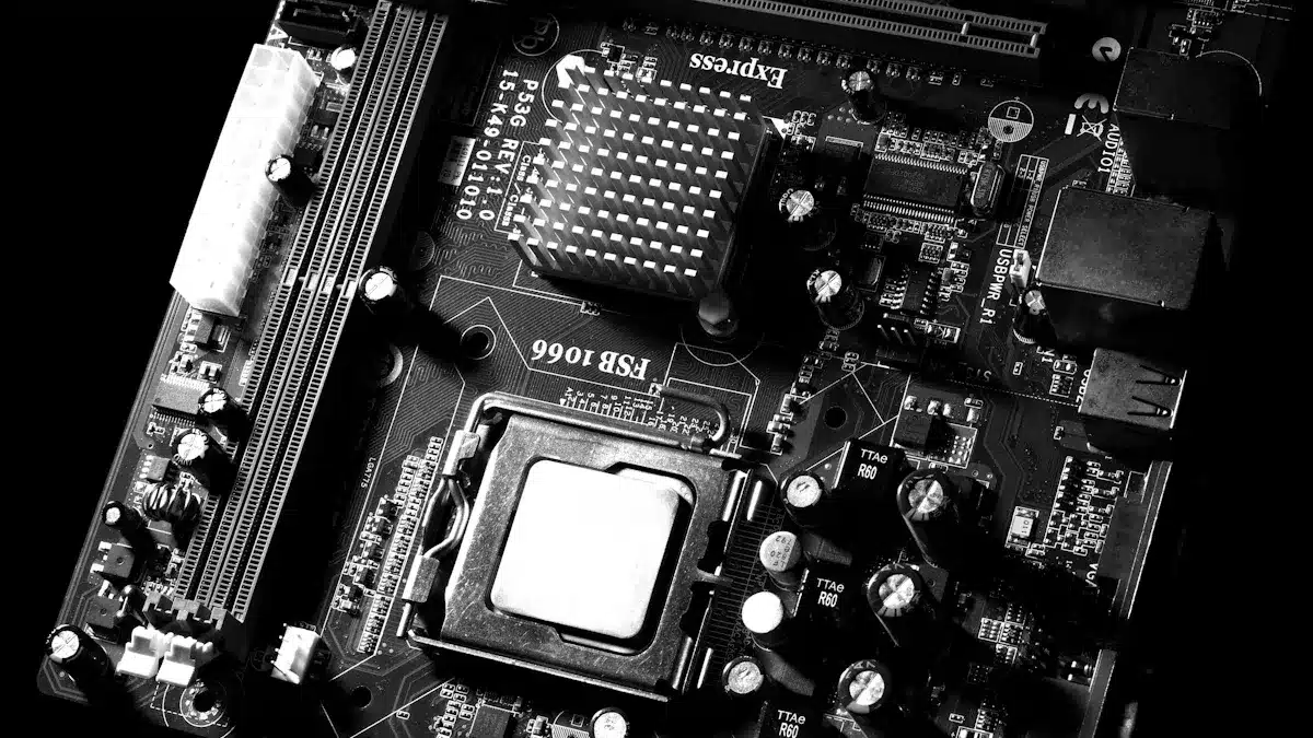
An electronic printed circuit board, or PCB, is the base of most modern electronics. A PCB has a hard base that does not conduct electricity. It has thin copper lines on it. These lines let electronic parts connect in a neat way. The printed circuit board took the place of messy wires. This made devices smaller and more reliable. Over time, better PCB design made gadgets lighter and faster. It also made them work better. The main job of PCBs is to hold and connect parts. This helps electronics work well.
Key Takeaways
Printed circuit boards (PCBs) hold and link electronic parts. They use copper lines on a base that does not conduct electricity. This makes devices smaller and more dependable.
PCBs have different types like single-sided, double-sided, multilayer, rigid, flexible, and rigid-flex. Each type fits certain device needs.
Good PCB design and routing help signals move quickly and clearly. This lowers noise and makes devices work better and last longer.
Making PCBs takes careful steps from design to putting parts together. Quality checks make sure boards work well and stay strong.
PCBs are very important in almost all modern electronics. They let smartphones, computers, cars, and medical devices do complex jobs.
Electronic Printed Circuit Board Basics
What Is a Printed Circuit Board
An electronic printed circuit board is the base for most electronics. It holds parts and connects them in a safe way. The board uses a hard base that does not let electricity pass. FR-4 is a common material for this base. It is strong and stops electricity from going where it should not. Thin copper traces are on the board’s surface. These traces are paths for signals. They link different parts together.
Printed circuit boards have many shapes and sizes. Some have one copper layer. Others have many layers stacked up. Multi-layer boards can hold more parts and make complex circuits. Engineers use pcb design to plan where traces and parts go. Good pcb design helps devices work faster and better.
Printed circuit boards do many important jobs in electronics:
Mechanical support: They give a strong base for parts.
Electrical connections: Copper traces send signals between parts.
Power distribution: The board sends power to each part.
Organization of complex circuits: Multi-layer boards fit many links in small spaces.
Hosting components: Both passive and active parts attach to the board.
Signal transmission and device control: Traces guide signals so parts can control voltage or switch functions.
Structural features: Layers, vias, solder masks, and silkscreens protect the board and help assembly.
Tip: Engineers use pcb design software to make layouts for each device. Careful planning helps printed circuit boards work well and last longer.
PCB Structure and Materials
A printed circuit board has several layers. The main part is the base. It does not let electricity pass. FR-4 is the most used base material. It is strong, insulates well, and resists heat and fire. Other materials like polyimide, metal-core, and ceramics are used for special needs. Polyimide is good for flexible boards. Metal-core boards use aluminum or copper to handle heat in strong devices. Ceramic boards resist heat and insulate well for tough jobs.
Key Properties | Typical Applications | |
|---|---|---|
FR-4 | Strong, flame retardant, stable | General electronics, multi-layer boards |
Rogers | Low signal loss, high thermal stability | High-frequency circuits, microwave devices |
Metal-Core | Great heat dissipation, lightweight | Power electronics, LED lighting |
Polyimide | Flexible, heat resistant | Flexible PCBs, harsh environments |
CEM | Cost-effective, moderate strength | Consumer electronics, simple boards |
PTFE | Chemically inert, high temperature | RF boards, microwave circuits |
Ceramic | Superior heat resistance, robust | Aerospace, military, high-power devices |
The material choice affects how well the board works. FR-4 is used most because it is strong and not expensive. Polyimide lets boards bend and fit tight spaces. Metal-core and ceramic boards handle high heat and power. Engineers pick materials based on what each device needs, like speed, heat, and cost.
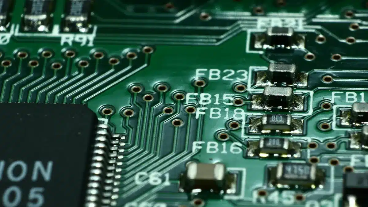
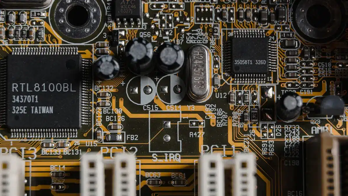
PCB structure has copper traces, solder masks, and silkscreens. Copper traces carry signals and power. Solder masks protect traces and stop short circuits. Silkscreens show where to put each part. Vias link layers and let signals move between them.
Printed circuit boards are the base for both mechanical and electrical needs in devices. They keep parts in place and make sure signals and power reach every part. Good pcb design and the right materials help boards last longer and work better, even in tough places.
PCB Components
Common Components on Printed Circuit Boards
Printed circuit boards have many electronic parts. Each part does something important. Some parts control how electricity moves. Other parts keep energy or change signals. Here are the most common components you will find:
Resistors: They slow down electric current.
Capacitors: They hold and let out energy. They help with timing and filtering.
Inductors: They keep energy in magnetic fields. They help with tuning and filtering.
Fuses: They stop too much current from hurting the circuit.
Integrated Circuits (ICs): They put many tiny parts into one chip. They do hard jobs.
Diodes: They let current go one way only.
Transistors: They act like switches or make signals stronger.
Silicon-controlled Rectifiers: They handle lots of voltage and current.
Crystal Oscillators: They give steady timing signals.
Sensors: They turn things like heat or light into signals.
Connectors: They join the pcb to other boards or devices.
Note: The number and kind of parts on a pcb depend on what the device needs to do.
How Components Connect on a PCB
A printed circuit board links parts with thin copper lines. These lines are like tiny roads for signals. Engineers pick where each part goes on the pcb. This helps signals move fast and safe. Copper lines join resistors, capacitors, and integrated circuits so they work together. This lets the pcb send signals, use power, and handle data.
Printed circuit boards have layers to fit more links in small spaces. Vias are tiny holes that let signals go between layers. Careful design keeps signals strong and cuts down noise. Good layout helps the board last longer and work better. The way parts work together on printed circuit boards lets devices do things like process data, make signals stronger, and control actions. Each part does its job, but together they make the whole system work.
How PCBs Work
Electrical Connections and Signal Flow
A pcb is like a map for electricity. Copper traces act as roads for signals. Signals start at a source, like a microchip or sensor. They travel along copper paths to other parts. Signals go through resistors, capacitors, and integrated circuits. These parts change, block, or boost signals.
Signals sometimes move between layers in the board. Vias are tiny holes lined with metal. They let signals go up or down between layers. Connectors on the edge let signals enter or leave the board. This links the pcb to other devices.
The way signals move on a pcb has steps:
They go through parts that change the signals.
Vias link traces between layers for vertical movement.
Connectors let signals come in or go out.
Signals can be digital, analog, or high-speed.
High-speed signals need special traces to stay clear.
Good routing avoids sharp bends and crosstalk.
Ground planes and shields block noise and interference.
Vias and connectors help stop signal loss.
Engineers use tricks to fix problems like noise.
Tip: A pcb transmission line has a signal trace and a return path. The return path is usually a ground plane. Keeping them close helps stop noise and keeps signals clean.
Routing and Functionality
Routing means planning how signals move across the pcb. Good routing helps the board work well and last longer. Engineers use different ways to make sure signals reach the right spot.
Differential pair routing keeps two traces close and equal in length. This lowers noise and keeps signals together.
Controlled impedance routing uses careful trace width and spacing. This stops signal reflections and keeps signals sharp.
Via optimization means using the right number and type of vias. Microvias and buried vias help high-speed signals move well.
Ground and power planes act as shields. They block noise and give signals a steady base.
Trace spacing is important. Keeping traces apart lowers crosstalk, which is unwanted noise.
Length matching makes sure signals arrive at the same time. This matters for fast circuits.
Avoiding sharp bends, like right angles, helps stop signal reflections.
Wider traces carry more current and help with heat.
A well-designed pcb uses these routing methods to work better. For example, microstrip and stripline routing put traces in special spots to control noise and speed. Engineers use decoupling capacitors near power pins to stop voltage spikes.
Routing Method | Purpose | Benefit |
|---|---|---|
Differential Pair | Match trace lengths and spacing | Lowers noise, keeps timing |
Controlled Impedance | Set trace width and spacing | Stops signal reflections |
Via Optimization | Use right type and number of vias | Keeps signals strong |
Ground/Power Planes | Add solid layers for reference | Blocks noise, helps with heat |
Trace Spacing | Keep traces apart | Lowers crosstalk |
Length Matching | Make traces the same length | Signals arrive together |
Avoid Sharp Bends | Use 45-degree angles | Stops signal reflections |
Note: Good routing and layout help a pcb handle fast signals, lower errors, and keep devices working well.
A pcb with smart routing and strong signal flow supports all the parts in a device. Careful planning lets electronics work fast, stay cool, and last longer.
Types of Printed Circuit Boards
Single-Sided and Double-Sided PCBs
Printed circuit boards can be single-sided or double-sided. A single-sided pcb has copper wiring on one side only. All the parts sit on that same side. This type works best for simple circuits like LED lights. It is also used in basic home appliances. Single-sided boards cost less and are easy to make. They cannot handle complex wiring.
Double-sided pcbs have copper wiring on both sides. Engineers use small holes called vias to link both sides. This lets parts go on both surfaces. The board becomes smaller and more efficient. Double-sided boards work for harder circuits. You find them in computers, smartphones, and cars. They give better signal performance and are more reliable.
Aspect | Single-Sided PCB | Double-Sided PCB |
|---|---|---|
Structure | Copper foil and wiring on only one side | Copper foil and wiring on both sides, connected via vias |
Component Placement | Components placed on one side | Components can be placed on both sides |
Circuit Complexity | Suitable for simple circuits | Supports complex circuit layouts |
Application Examples | LED lights, household appliances | Computers, smartphones, automotive systems |
Manufacturing Cost | Lower cost, simpler process | Higher cost, more complex manufacturing |
Board Size | Larger size due to wiring crossing limitations | Smaller size due to efficient wiring on both sides |
Signal Performance | Limited signal transmission capability | Improved signal transmission and circuit performance |
Wiring Flexibility | Limited, single-layer wiring | Flexible wiring, easier debugging and maintenance |
Reliability | High reliability for simple circuits | More reliable connections via through-hole plating |
Double-sided pcbs fit more parts and handle heat better. This makes them great for advanced electronics.
Multilayer Printed Circuit Boards
Multilayer pcbs have three or more layers stacked together. These boards fit lots of parts and wires in a small space. Engineers use multilayer pcbs in fast and powerful devices. You see them in smartphones, tablets, and medical equipment.
Advantages of multilayer pcbs:
They improve signal quality and cut down interference.
They allow small designs for tiny devices.
They have special layers for power and ground, which helps stability.
Disadvantages of multilayer pcbs:
They cost more to make because they are complex.
They take longer to build and need skilled workers.
They are harder to fix since layers are hidden.
They need careful design to avoid problems.
Aspect | Multilayer PCBs Disadvantages | Single-Layer PCBs Advantages | Single-Layer PCBs Disadvantages | |
|---|---|---|---|---|
Complexity | Can handle more complex functionality | More complicated design and production requiring skilled designers and equipment | Simpler design and production, easier to manufacture | Too simplistic for complex projects |
Quality and Performance | Higher quality, more power, speed, and operating capacity | More complex repairs due to hidden layers and numerous components | Consistent positive results due to simplicity | Lower operating capacity and slower speed |
Size and Weight | Smaller size and reduced weight | Limited availability of manufacturers and longer lead times | Larger size and higher weight due to limited layering | Larger size and higher weight |
Cost | N/A | Higher costs due to complexity and production time | Lower cost due to simpler production | N/A |
Repair and Maintenance | N/A | More complex repairs and troubleshooting | Easier repairs due to simpler design | N/A |
Production Volume | N/A | N/A | Can be produced at high volume | N/A |
Multilayer pcbs make electronics smaller, faster, and stronger. They need careful planning and skilled workers to build.
Rigid, Flexible, and Rigid-Flex PCBs
Printed circuit boards can be rigid, flexible, or both. Rigid pcbs use strong materials like FR-4 fiberglass. These boards keep their shape and hold heavy parts. Rigid pcbs are used in machines and power electronics.
Flexible pcbs use bendable materials like polyimide. These boards twist and fold to fit tight spaces. Flexible pcbs are found in wearables, cameras, and cars. They absorb shocks and handle high heat.
Rigid-flex pcbs mix both types. Some parts stay stiff, while others bend. This lets engineers fit circuits into small or odd spaces. Rigid-flex pcbs need fewer connectors and cables. This makes them more reliable. They are used in medical devices, military gear, and airplanes.
Aspect | Rigid PCBs | Flexible PCBs | Rigid-Flex PCBs |
|---|---|---|---|
Materials | FR-4 fiberglass substrate; stable, cost-effective | Polyimide substrates; flexible, maintain electrical integrity under stress | Combination of rigid (FR-4 or polyimide) and flexible materials; complex selection |
Manufacturing | Mature, standardized, high-volume, cost-effective | Specialized equipment and processes; higher setup cost | Complex; requires early collaboration with manufacturers for material and design choices |
Typical Use Cases | Applications needing rigidity, thermal management, mechanical stability (e.g., industrial control, power electronics) | Compact, lightweight, dynamic applications (e.g., consumer electronics, aerospace, automotive) | High-performance, space-constrained, demanding environments (e.g., medical implants, military, aerospace) |
Cost Considerations | Lower initial cost due to economies of scale | Higher initial cost but can reduce system-level costs by eliminating connectors | Moderate cost; reduces connectors and cables, improving reliability |
Design Considerations | Focus on thermal management, signal integrity, manufacturability | Mechanical reliability, bend radius, trace thickness, stress reduction | Integration of rigid and flexible sections; optimized for bending and thermal stability |
Engineers pick the right pcb type based on what the device needs. They look at strength, flexibility, and space.
How Are PCBs Made
Design and Layout
Engineers begin by learning what the device needs. They check how much current and voltage it uses. They also look at what signals are needed. They decide where each part should go. First, they draw a simple block diagram. Then, they make a schematic to show how parts connect. They use pcb design software like Altium Designer, OrCAD, or KiCad. These programs help plan the board and check for mistakes. They also help with routing and signal checks.
The pcb design process has many steps. First, engineers pick where parts will go. Next, they draw the schematic using special tools. They check if all parts are easy to get. They plan how many layers the board needs. They set the shape of the board and put parts in place. Then, they draw copper lines to link everything. They add labels and marks for assembly. Last, they make files for the factory to use.
Engineers follow rules for spacing and trace width. They also check how many layers are needed. Design rule checks help find mistakes before making the board.
Software Tool | Key Features |
|---|---|
3D views, teamwork, easy routing | |
OrCAD | Circuit checks, signal tests |
KiCad | Free, open-source, checks for errors |
Fabrication Steps
Making a pcb turns the design into a real board. The process starts with a review to catch mistakes. Factories print films for each layer and solder mask. They cover the board with a special coating. UV light makes the copper stick in the right spots.
Here are the main steps to make a pcb. First, print films and line up the layers. Next, put on photoresist and shine UV light. Then, remove extra copper that is not needed. Layers are pressed together with heat. Holes are drilled for parts and connections. Copper is added inside the holes. A solder mask and silkscreen are put on. A surface finish is added to protect the board. At the end, the board is checked and tested.
Every step must be very exact. Small mistakes can cause big problems. Multi-layer boards need careful lining up. Fixing a pcb is hard, especially with tiny parts. Workers use microscopes and special tools to fix boards.
Assembly and Quality Control
After making the board, workers put parts on it. Machines help place and solder each part. Quality control makes sure the board works well. Solder Paste Inspection checks if paste is in the right spot. Automated Optical Inspection looks for missing or wrong parts. X-ray Inspection checks hidden solder joints. Functional testing makes sure the board works like it should. In-Circuit testing checks each part for problems.
Clean rooms keep dust away from boards. ESD-safe areas stop static from hurting parts. Supply chain checks make sure parts are real. Skilled workers and good machines help find problems early. Fixing a pcb can be slow and hard. Small parts and heat-sensitive boards need gentle care.
Tip: Careful pcb design and strong testing help devices last longer and work better.
PCB Applications
Everyday Devices Using PCBs
Printed circuit boards are inside almost every electronic device. They help control, connect, and power many things we use. You can find them at home, at work, and in cars. Here are some examples:
Computers and laptops
Televisions and gaming consoles
Wearable devices such as fitness trackers and smartwatches
Home appliances like refrigerators and washing machines
Automotive electronics, including engine control, audio, digital displays, radar, ABS, air conditioning, steering, LED lights, dashboards, navigation, and engine timing
Printed circuit boards help devices manage signals, store data, and connect online. In smartphones, they organize many jobs, like calling and running apps. Home appliances use them to control how they work and check their performance. Wearable devices need small, bendy printed circuit boards for sensors and wireless features. Almost every electronic device has a printed circuit board that lets it send signals and do important jobs.
Did you know? In 2024, companies made billions of printed circuit boards for electronics. Over 1.5 billion smartphones and tablets were shipped, each with at least one printed circuit board inside.
Importance in Modern Electronics
Printed circuit boards are very important for modern electronics. Engineers use advanced printed circuit board design to arrange parts and circuits. This helps with power, signal quality, and heat control. Careful planning lets devices get smaller, faster, and more reliable. New materials, like special bases and conductive inks, help printed circuit boards work better in fast and flexible electronics.
Modern printed circuit boards support strong processors, memory, and communication parts in smartphones and laptops. They use multilayer designs, vias, solder masks, and surface finishes to keep signals clear and devices strong. These features let engineers fit more functions into smaller spaces. This helps new ideas in aerospace, telecommunications, and car electronics.
Some big changes made possible by printed circuit board technology are:
Double-sided and multilayer printed circuit boards for complex circuits in small devices
Surface Mount Technology for smaller, more reliable products
High-Density Interconnect for compact, high-performance electronics
Flexible and rigid-flex printed circuit boards for bendy and wearable devices
Safer materials and finishes for better production
3D printed electronics and built-in parts for faster testing
Where do people use printed circuit boards? They are in medical devices, imaging machines, military gear, and aerospace systems. The electronics industry needs printed circuit boards for good, low-cost work and new inventions.
PCB Feature | Impact on Modern Electronics |
|---|---|
Multilayer design | Helps make devices smaller and complex |
Advanced materials | Makes devices last longer and work well |
Surface finishes | Improves safety and reliability |
Flexible construction | Lets devices bend and fold |
Printed circuit boards are very important in electronics today. They hold and link all the parts in a device. This helps make gadgets smaller, quicker, and more dependable. PCBs started as simple boards many years ago. Now, they are much more complex and packed with parts. You can find them in things like phones, cars, and medical equipment. Their design lets parts connect safely and work well together. PCBs also help new trends like tiny gadgets and bendy electronics. As technology gets better, PCBs stay a key part of every device. They have a lot going on inside, even if you cannot see it. 🛠️
FAQ
What does a PCB do in an electronic device?
A PCB holds parts in place. It connects them with copper lines. These lines help signals and power move around. The board keeps everything neat and safe.
Why do engineers use different materials for PCBs?
Engineers choose materials for each device’s needs. FR-4 is used for most boards. Polyimide bends for flexible boards. Metal-core helps with heat. Each material has its own good points.
Can someone repair a damaged PCB?
Fixing a PCB is not easy. The parts are small and lines are thin. Skilled workers use special tools to fix or replace broken parts.
How do PCBs help make devices smaller?
PCBs have layers and tiny copper lines. This lets many parts fit in a small space. Engineers can make small gadgets like phones and watches.
Are PCBs safe for the environment?
Factories use safer materials and recycle more now. Many companies follow rules to cut waste and pollution. Some boards use lead-free solder to help people and nature.
See Also
Exploring The Definition And Function Of PCBA In Devices
Understanding The Meaning And Purpose Of PCBA In Electronics
Why PCBA Matters And What It Means In Electronics