
Precision is very important when making high-performance GPU PCBs. Small mistakes during production can cause problems and hurt GPU performance. For example, advanced chip technologies need exact manufacturing for fast data transfer. This is key for GPUs to work well. Research shows better models can find 99.5% of open circuit issues. This proves careful processes are necessary. Also, heat tests on NVIDIA GeForce RTX 50 series PCBs show bad precision can cause temperatures over 100°C. This shows why good design matters. Every step in GPU PCB assembly needs great accuracy for the best results.
Key Takeaways
Making GPU PCBs needs great care. Small mistakes can cause problems, so good planning and testing are very important.
Picking the right materials makes PCBs work better. Use materials that handle heat well and connect electricity strongly.
Putting on solder paste correctly is important. Use stencils to be precise and spread the paste evenly to stop mistakes.
Checking and cleaning often keeps PCBs working well. Machines can find problems early, helping make better products.
Testing in real-life situations is important. Heat and stress tests show if the PCB can do tough jobs without breaking.
PCB Manufacturing Process
Design and Prototyping
Design and prototyping are the first steps in making a PCB. A schematic is created to show how parts connect and fit together. This helps ensure all components are placed and linked correctly. Modern tools let you test how the PCB will work before making it. This helps find problems early.
To make better PCBs, follow these tips:
Careful Component Selection: Pick parts that work well for powerful GPUs, like those used in AI.
Address Thermal Management: Add systems to keep the PCB cool and avoid overheating.
Improve Signal Integrity: Design traces carefully and use shields to keep signals clear.
Use Rapid Prototyping: Test designs quickly to save time and speed up production.
Smaller and faster PCBs are in high demand. New designs, like HDI, are helping meet this need. These designs are used in IoT and 5G devices. Over five years, HDI use grew from 37.5% to 49%, showing the move toward smaller, better PCBs.
Material Selection
Picking the right materials is key for making good GPU PCBs. You need materials that handle heat, work well with electricity, and stay strong. Good heat conductivity keeps the PCB cool. Low dielectric constant and loss tangent help signals stay clear. Strong materials make sure the PCB lasts under stress.
Here are important material features to consider:
Trace Quality and Layout: Helps data move fast and keeps signals clear.
Power Delivery System (VRMs): Keeps the PCB stable during heavy use or overclocking.
Cooling Solutions: Prevents overheating and helps parts last longer.
Layer Count and Thickness: Affects heat control and signal clarity.
Ground Plane Design: Reduces interference and improves signal quality.
The PCB industry is growing fast. Flexible PCBs and roll-to-roll methods are boosting production. In 2023, the industry was worth $9 billion. It’s expected to grow by 10% yearly from 2024 to 2032.
Substrate Preparation
Substrate preparation is an important step in making PCBs. The substrate is cleaned to remove dirt and ensure layers stick well. This step helps keep the PCB strong and high-quality.
High-density PCBs, like those in GPUs, need careful preparation. Research shows these steps:
Step | Description |
|---|---|
1 | Remove water at 30 °C under vacuum for 40 minutes. |
2 | Dry at 80 °C under vacuum using metal plates for 40 minutes. |
3 | Finish the surface at 120 °C using polished plates for 15 minutes. |
These methods prepare the substrate for fast and high-frequency use. Using tools like SPC has improved production results. One company saw an 18% improvement in three months after using SPC. This shows how precision helps in this step.
Photolithography and Etching
Photolithography and etching are key steps in making PCB patterns. In photolithography, a light-sensitive material called photoresist is added to the PCB. A mask with the circuit design is placed on top. Ultraviolet (UV) light shines through the mask, hardening the exposed photoresist. The soft, unexposed parts are then removed. This step creates the exact paths for the circuits.
Next comes etching. Chemicals remove extra copper from the PCB, leaving only the circuit paths. The hardened photoresist protects these paths during this process. This step is important for making the tiny lines that connect parts on the board. New methods, like plasma etching, make this process more accurate and waste less material.
To get the best results:
Use advanced UV systems for better precision.
Apply photoresist evenly to avoid mistakes.
Watch the etching process to prevent errors.
Photolithography and etching are crucial for high-density PCBs, like those in GPUs. These steps create the detailed paths needed for fast data movement between parts.
Surface Finishing
Surface finishing is an important step in making a PCB. It protects the board’s outer layers and prepares it for assembly. Without it, the copper parts could rust, causing poor connections and lower performance.
Why is surface finishing so important? It shields the PCB from things like moisture and harmful gases. These can damage the board over time. A good finish makes the board last longer. It also helps parts stick better during soldering. This prevents problems like weak joints or missing connections, which can make the PCB fail.
There are different types of surface finishes for PCBs. Each works best for certain uses. Here are some common ones:
HASL (Hot Air Solder Leveling): Cheap and gives strong protection.
ENIG (Electroless Nickel Immersion Gold): Resists rust and suits high-performance boards.
OSP (Organic Solderability Preservative): Lead-free, eco-friendly, and good for simple designs.
Immersion Tin or Silver: Flat surface for soldering, used in dense PCBs.
When picking a surface finish, think about where the PCB will be used. For tough conditions, ENIG is a strong choice. Advanced finishes not only protect the board but also improve its performance. They help handle fast signals without issues, which is vital for GPUs.
To get the best results, manufacturers use careful methods. They apply the coating evenly and check its thickness. These steps keep the PCB reliable and high-quality. Picking the right finish ensures the board works well and lasts a long time.
GPU PCB Assembly Process
Solder Paste Application
The first step in assembling a GPU PCB is applying solder paste. This paste is placed on the PCB pads where parts will go. A stencil, matching the PCB design, helps apply the paste only to the right spots. This ensures accuracy and neatness.
Good solder paste application is very important. It affects how well the PCB works. High-quality paste should work well even with different printing speeds or pauses. Research shows that using a stencil with a small opening area (<0.66) gives better results. This keeps the GPU PCB reliable and consistent.
Description | |
|---|---|
Print Performance | High paste amounts and low errors mean better application. |
Print Speed Variation | Paste works well even with printing pauses. |
Reflow Performance | Checks for strong connections by testing solder wetting and balling. |
Overall Scoring | Rates solder pastes based on results from many tests. |
To get the best results, keep the stencil clean and lined up with the PCB. Machines can help make this process more accurate and reduce mistakes. This step is key to starting the assembly process right.
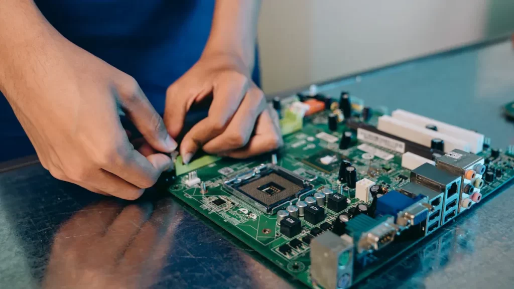
Component Placement
After the solder paste is applied, parts are placed on the PCB. This step needs to be very precise. Even small mistakes can hurt the GPU’s performance. Machines called pick-and-place are used to put parts in the right spots. These machines use cameras to find the exact positions.
Placing parts correctly is very important for the PCB to work well. For example, putting parts in the right spots reduces power loss and signal problems. It also makes the PCB stronger, so heavy parts don’t cause damage.
Description | |
|---|---|
Power Distribution | Helps the PCB handle high currents without overheating. |
Signal Integrity | Keeps data moving fast and stable by controlling wiring. |
Thermal Management | Uses features like copper areas to remove heat from the GPU. |
Component Placement | Reduces power loss and signal issues by placing parts smartly. |
Mechanical Stability | Makes the PCB strong enough to handle stress from heavy parts. |
You can improve this step by using tools to test part placement before assembly. These tools find problems early, saving time and effort.
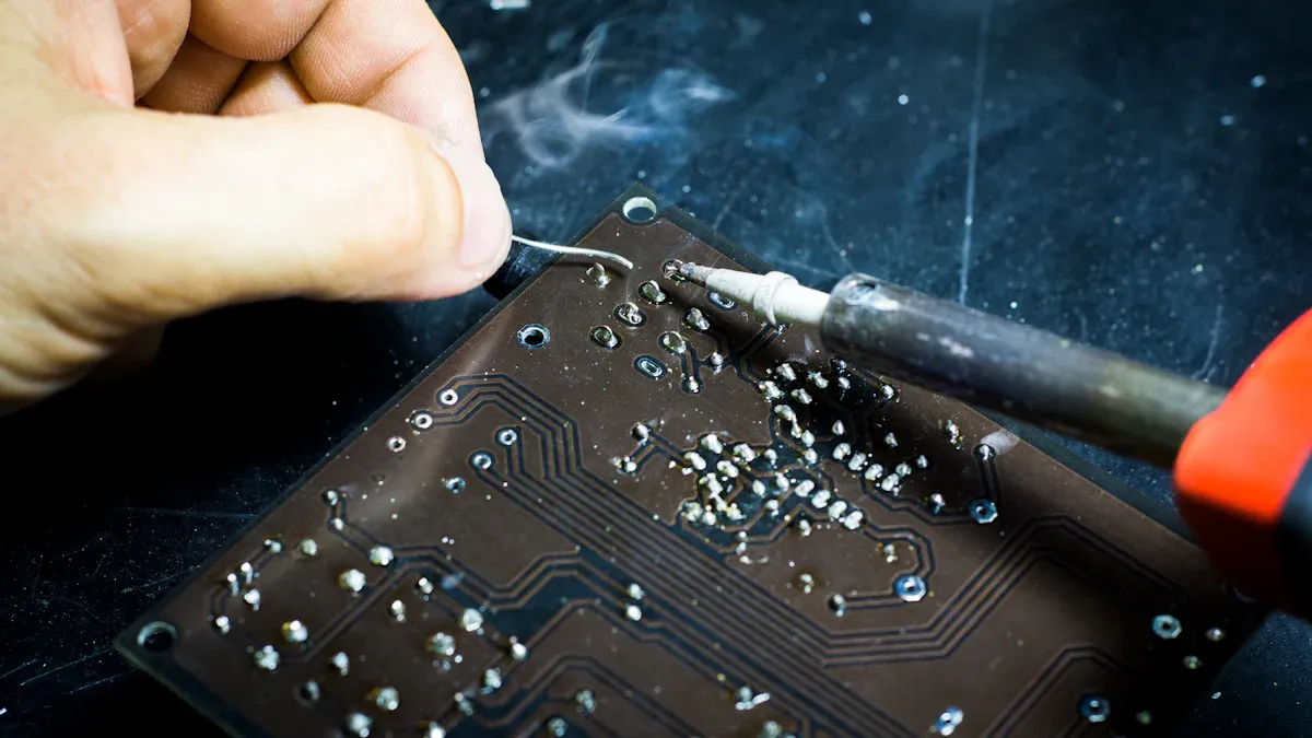
Reflow Soldering
Reflow soldering is the last step to attach parts to the PCB. The PCB goes through a special oven where heat melts the solder paste. This creates strong bonds between the parts and the PCB. This step is very important for making sure the GPU PCB lasts a long time.
Machines make reflow soldering more precise, but the solder material also matters. Lead-based solder works well but has issues with heat stress in lead-free options. This stress can weaken solder joints and cause problems. Studies show that solder balls like SAC305 can wear out from heat and cooling cycles. This can harm the PCB’s strength.
To avoid these problems, watch the reflow process closely. Control the oven’s heat and timing carefully. Good reflow soldering ensures the GPU PCB can handle tough tasks without losing quality.
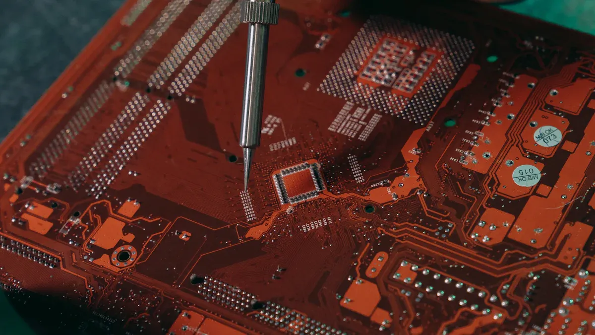
Inspection and Cleaning
Inspection and cleaning are important for making sure GPU PCBs work well. After putting the board together, it is checked for mistakes or problems. Machines called automated optical inspection (AOI) systems help with this. These machines use cameras and smart programs to check solder spots, part placement, and overall board quality. AOI makes sure every PCB meets the needed standards before moving forward.
Cleaning comes after inspection and removes leftover materials from soldering. Things like flux residue can cause problems later, such as rust or electrical shorts. Cleaning makes the PCB more reliable and helps it work better in different situations. Special cleaning tools and liquids are used to get good results.
Below is a table showing key inspection and cleaning steps and how they improve PCB quality:
Procedure Type | Description | Impact on Yield Enhancements |
|---|---|---|
Final Testing | AOI checks solder spots and part placement. | Ensures quality before shipment |
Environmental Testing | Tests how the PCB handles different conditions. | Reduces failure rates |
Post-Assembly Cleaning | Removes leftover soldering materials for better reliability. | Improves circuit lifespan |
Tight Process Control | Keeps cleaning quality steady across designs. | Boosts overall yield |
Using these steps makes the PCB stronger and longer-lasting. Regular checks and cleaning make sure the board is ready for the next stage.
Final Assembly and Integration
Final assembly and integration put all GPU PCB parts together. This step adds extra pieces like heatsinks, connectors, and covers to finish the board. Careful work is needed here. Good soldering and correct placement of parts make sure the PCB works properly.
Testing is very important during this step. It checks how the PCB handles real-world conditions. For example, heat tests show if the PCB can deal with the heat it creates while working. Keeping the same quality for every PCB is also key. This ensures all boards are reliable and meet customer needs.
Here are some things that help with final assembly and integration:
Good soldering and part placement make the PCB reliable.
Testing finds problems by copying real-world conditions.
Keeping quality steady across batches ensures all boards are the same.
Following rules like ISO 9001 shows a focus on quality.
By doing these things, you can make a GPU PCB that works well for tough tasks like gaming or AI. Final assembly and integration make sure the board is ready to perform without issues.
Quality Assurance and Testing
Visual Inspection
Visual checks are important for making sure GPU PCBs are good. This step finds problems early, stopping issues that could hurt performance. Machines like ACASEM models are often used for this task. These machines use smart programs to spot tiny flaws with great accuracy.
Why visual checks work well:
Figures 10 and 11 show all models found defects confidently.
No flaws were missed or wrongly labeled, ensuring strong quality control.
ACASEM models showed better accuracy for small flaws, proven by higher AP_s and AR_s scores.
Using these tools makes sure every PCB meets high standards before moving forward. This step is key for keeping GPU PCB production reliable and consistent.
Functional Testing
Functional testing checks if the GPU PCB works as it should. This step tests how the board handles signals, power, and data. Special machines copy real-world conditions to see if the PCB works properly.
For example, tests check if the PCB can handle fast data and power changes. This helps find weak spots in the design. Functional testing also makes sure the PCB can handle tough tasks like gaming or AI work.
You can make this step better by using tools to measure signal clarity and power steadiness. These tools confirm the PCB meets performance needs before the final checks.
Thermal and Stress Testing
Thermal and stress tests check if the GPU PCB stays strong in tough conditions. These tests look at how the board handles heat, moisture, and physical stress. They make sure the PCB stays reliable over time.
Common test types include:
Test Type | Purpose |
|---|---|
Checks if PCBs last long in electronic devices. | |
High Accelerated Temperature and Humidity Stress Testing (HAST) | Tests if PCBs handle heat and moisture well. |
Temperature Cycling Testing | Checks PCB strength under changing temperatures. |
Salt Spray Testing | Tests PCB resistance to rust in salty conditions. |
These tests measure how tough the PCB is. By doing these checks, you make sure the GPU PCB works well in hard environments. This step is very important for keeping the final product reliable and high-quality.
Reliability and Longevity Testing
Reliability and longevity tests check if a GPU PCB works well over time. These tests copy real-world conditions to find weak spots. This helps ensure the PCB stays reliable, even with heavy use.
One key test is thermal cycling. It heats and cools the PCB repeatedly, like what happens during use. For example, when a GPU handles tough tasks, it gets hot. If the PCB can’t handle these changes, it might break early. Another test is vibration testing, which checks if the PCB can handle shaking or bumps. This is important for GPUs in gaming or factories, where vibrations happen often.
PCB quality control is a careful process that covers every step of production. It starts with making sure the design is easy to build and includes checking materials for quality. Manufacturing steps must be precise, and inspections happen at many levels. Even small steps, like via plugging, can hide risks. Problems like trapped air or leftover chemicals can cause failures later, such as broken circuits. These issues can hurt reliability and user experience.
To make PCBs more reliable, humidity resistance testing is also important. This test checks if the PCB can handle moisture, which can cause rust or shorts. Another test, salt spray testing, looks at how well the PCB resists rust in salty air. These tests help the PCB last longer and work better.
Regular checks during testing catch problems early. For example, machines can find weak solder spots or bad connections. Fixing these issues improves the PCB’s reliability and ensures it meets high standards.
Making a GPU PCB needs careful steps, from design to assembly. Each part, like photolithography or soldering, helps the PCB work well. Checking for mistakes early is important for reliability. Accurate PCB-making has big benefits, even in health care. GPUs help calculate cancer treatment doses quickly using particle beams. This shows how better PCB technology leads to new ideas. By focusing on precision, you help create GPUs for gaming, AI, and science.
Feature | Details |
|---|---|
Medical Use | |
System | FRoG (Fast Recalculation on GPU) |
Beam Types | Proton, helium, carbon, and oxygen |
Speed | Fast dose calculations in just minutes |
Accuracy | Matches top-level Monte Carlo simulation standards |
Purpose | Compares models to estimate effective doses in 3D |
Making precise PCBs not only keeps GPUs reliable but also helps improve many industries.
FAQ
What does a GPU PCB do?
A GPU PCB holds and connects the parts of a graphics card. It helps deliver power, send signals, and manage heat. This allows the GPU to handle tasks like gaming, AI, and video editing.
Why is managing heat important in GPU PCBs?
Managing heat stops parts from overheating, which can cause damage. Features like copper layers and heatsinks help cool the GPU. This keeps it working well during heavy use.
How do makers check PCB quality?
Makers use machines to inspect, test, and stress the PCB. These steps find problems, check how it works, and ensure it handles real-world use. Good checks make the PCB last longer and work better.
What materials are used for GPU PCBs?
GPU PCBs often use FR4, a strong and heat-resistant material. For better performance, some use polyimide or ceramic, which handle heat and electricity well.
Can GPU PCBs be reused?
Yes, GPU PCBs can be reused. Special centers recover useful materials like copper and gold. They also safely get rid of harmful waste. Recycling helps reduce trash and save resources.
💡 Tip: Always recycle old electronics at certified e-waste centers to protect the environment.
See Also
A Detailed Overview of the PCBA Production Process
Understanding the SMT Process in PCBA Assembly
An In-Depth Look at PCBA Manufacturing Procedures