
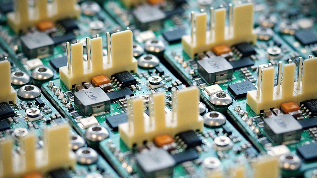
High-density interconnect (HDI) PCBA technology is a special type of circuit board. It features many layers and tightly packed connections. This design allows you to incorporate more components in less space without compromising performance.
HDI PCBA are crucial in today’s electronics. They enable the creation of smaller, lighter, and faster devices that still function exceptionally well.
With HDI PCBA, you can achieve compact designs that perform efficiently. This makes them essential for innovative and advanced technologies.
Key Takeaways
HDI PCBs help make devices smaller, lighter, and faster.
Tiny holes and smart wiring improve signals and reduce losses.
This makes HDI PCBs great for powerful electronics.
HDI technology makes devices more reliable in many industries.
Picking good materials and designs is very important.
Working with makers during design helps lower costs and improve quality.
How High-Density Interconnect (HDI) PCBs Work
Key Features of High-Density Interconnect
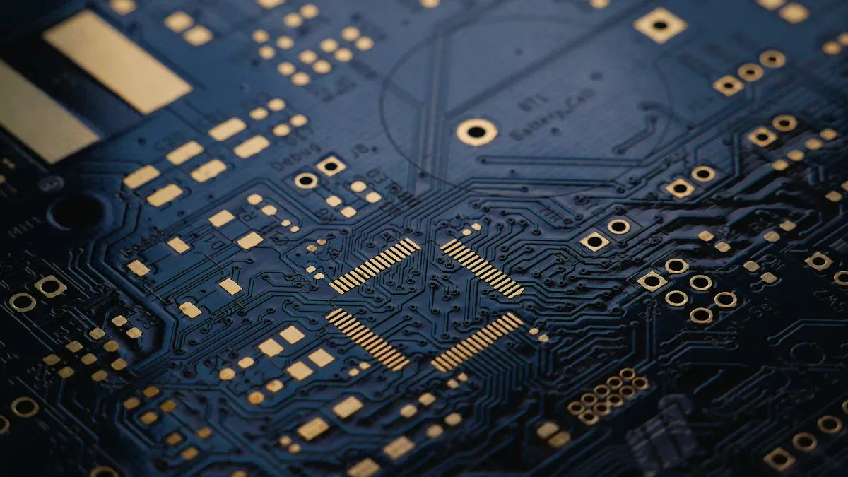
High-density interconnect PCBs are special because of their smart design. They have many layers and tightly packed connections. This helps them work well in small spaces. HDI PCBs use advanced methods like microvias, blind vias, and buried vias. These methods allow more circuits and better performance.
Some important features of HDI PCBs are:
Microvias: Tiny holes link layers, fitting more parts in less space.
High Routing Density: They handle more connections in smaller areas than regular PCBs.
Improved Signal Integrity: Smaller gaps and better materials reduce signal loss and improve performance.
These features make HDI PCBs perfect for small, powerful devices like phones, medical tools, and cars.
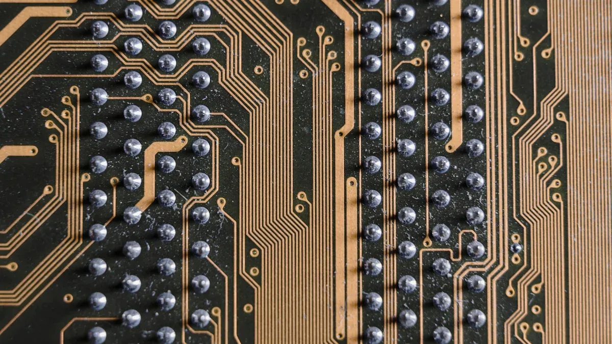
Microvias, Blind Vias, and Buried Vias
Using microvias, blind vias, and buried vias is key to HDI PCB design. Each type connects PCB layers differently to save space and boost performance.
Via Type | What It Does | Benefits |
|---|---|---|
Microvias | Tiny holes link nearby layers. | Help fit more circuits and reduce signal loss. |
Blind Vias | Holes link outer layers to inner ones without going through the board. | Save space and make routing easier. |
Buried Vias | Holes link only inner layers, staying hidden from the surface. | Allow complex designs without affecting the outside layers. |
Microvias are very important for HDI PCBs. They allow smaller holes and tighter layouts, increasing wiring density. But they need precise laser drilling to work well. Blind and buried vias also save space but make the manufacturing process harder.
Compact Design and High Wiring Density
HDI PCBs are great for small designs with lots of wiring. They use smart methods like microvias and multi-layer setups. This helps fit more parts into tiny spaces. This is useful for devices like smartphones, where space is tight but performance matters.
HDI PCBs can fit 20% more parts than regular PCBs.
Microvias and buried vias help create detailed designs with less signal loss.
Multi-layer HDI designs, like in Tesla’s Battery System, show how HDI handles tough tasks.
HDI PCBs save space and improve performance. They reduce signal delays and keep signals strong. This makes them a top choice for high-tech electronics.
Benefits of High-Density Interconnect (HDI) PCBs
Smaller Size and Better Space Use
HDI technology changes circuit boards by making them much smaller. It lets you fit more parts into tiny spaces without losing performance. This is very important for gadgets like smartphones and smartwatches, where small size matters a lot.
Tiny holes, called microvias, help make this possible. These holes are less than 150 micrometers wide. They connect layers tightly, allowing more parts to fit. This increases how much you can do with the space on the board.
Microvias are key to HDI PCBs, helping save space and add more parts.
Some important points about smaller size and better space use are:
People want faster, stronger, and smaller devices, so HDI is needed.
HDI is very different from old-style boards, making better gadgets possible.
New PCB designs help create cool tech like AI and smart cars.
Feature | What It Means |
|---|---|
Making the Board | Special methods focus on small size and complex designs. |
Microvias | Tiny holes allow more parts and better use of space. |
Testing for Quality | Careful checks make sure the board works well in modern devices. |
Better Electrical Performance
HDI PCBs work better than regular circuit boards. They keep signals strong, which is important for fast data transfer. Microvias and thin lines help reduce signal problems, making them reliable even for tough tasks.
Feature | HDI PCBs | Regular PCBs |
|---|---|---|
Flexible Design | Better | Okay |
Signal Strength | Stronger | Normal |
Trace Amount | More | Fewer |
HDI PCBs meet high standards for electrical work. They are great for things like phone networks and smart car systems. With HDI, you get faster data and more reliable devices.
More Circuits in Less Space
HDI PCBs are great at fitting lots of circuits in small areas. Using microvias, blind vias, and buried vias, they allow detailed designs with many parts. This makes them perfect for small but powerful devices.
Feature | HDI PCBs | Regular PCBs |
|---|---|---|
Microvias | Yes | No |
Blind/Buried Vias | Yes | No |
Thin Lines | Yes | Limited |
Advanced stacking methods in HDI PCBs add even more circuits. Multi-layer designs let you fit more parts while keeping performance high. This is why industries like healthcare, space, and electronics prefer HDI PCBs.
Better Signal Quality
Signal quality is very important for modern devices to work well. High-density interconnect (HDI) PCBs are great at keeping signals strong. They use smart methods like microvias and special routing to avoid signal loss.
One big benefit of HDI is shorter signal paths. Shorter paths mean less resistance and fewer problems with signals. HDI also removes unused parts of vias, called via stubs. These stubs can cause signal issues, so removing them makes signals cleaner.
Another key feature is controlled routing for signals. This keeps signals steady and avoids problems like distortion or data loss. HDI often uses special materials called low-Dk laminates. These materials help signals move faster and stay strong.
Here’s a table showing how HDI improves signal quality:
Feature | Benefit |
|---|---|
Shorter Signal Paths | Better signal quality with less resistance and delay. |
No Via Stubs | Stops signal problems, making transmission cleaner. |
Controlled Signal Routing | Keeps signals steady for reliable performance. |
Low-Dk Laminates | Helps fast signals and reduces signal loss. |
HDI PCBs also have many layers, which help route signals better. The compact design means signals travel shorter distances. This reduces delays and boosts performance. HDI is perfect for fast devices like phones and computers.
Using microvias and smart designs, HDI keeps signals strong. These features make sure devices work well, even in tough conditions. Whether it’s a phone, medical tool, or car system, HDI gives the strong connections needed for great signal quality.
Applications of High-Density Interconnect (HDI) PCBs
Consumer Electronics
HDI PCBs are very important in today’s gadgets. Devices like phones, tablets, and smartwatches use them. These devices need to be small but work well. HDI technology helps make this possible. Using tiny holes and layers, HDI PCBs fit more parts in less space. This allows sleek designs without losing speed or quality.
More people want smarter and better gadgets. This increases the need for HDI PCBs. They help devices transfer data faster and use power better. HDI also keeps signals strong, making it perfect for advanced electronics.
HDI PCBs make gadgets smaller, faster, and more powerful.
Automotive Systems
Cars are getting smarter with HDI PCBs. They are used in safety systems, electric cars, and entertainment features. HDI PCBs make driving safer and cars more connected. Their strong design handles complex tasks easily.
Tiny holes in HDI PCBs help car systems process data quickly. For example, cameras and sensors in safety systems use them. Electric cars also depend on HDI PCBs for managing batteries and power.
Self-driving and connected cars need HDI PCBs. They are tough and reliable, making them perfect for modern vehicles.
Medical Devices
HDI PCBs are changing healthcare tools. They are used in health trackers, testing machines, and remote care devices. These tools need to be small and work well. HDI PCBs make this possible.
Tiny holes and layers in HDI PCBs allow smaller medical devices. For example, health trackers use them to check vital signs accurately. Testing machines benefit from faster data and better signals.
Remote healthcare depends on HDI PCBs. They help devices stay small and reliable. This makes HDI PCBs very important in improving healthcare.
HDI PCBs help medical tools work better, improving patient care and innovation.
Telecommunications Infrastructure
Telecommunications systems need advanced tech to manage lots of data. HDI PCBs are very important in this field. They help transfer data faster and keep signals strong. You can find them in routers, switches, and base stations.
One big benefit of HDI PCBs is handling high-frequency signals. Shorter paths and special materials reduce interference. This makes them perfect for 5G networks, where speed matters. With HDI, networks work better and stay connected.
Another advantage is their small size. Telecom equipment needs tiny, light parts to save space. HDI PCBs use microvias and layers to make compact devices. This helps meet the need for smaller, stronger communication tools.
Tip: Use HDI PCBs in telecom designs for better performance and space-saving.
Aerospace and Defense
Aerospace and defense need tough and reliable technology. HDI PCBs are great for these industries. They are used in radars, navigation tools, and communication systems for planes and military.
HDI PCBs are strong and handle tough conditions. They work well in heat, vibrations, and harsh places. For example, satellites use HDI PCBs to keep signals clear in space.
They also manage complex circuits. Aerospace and defense tools need fast data and precise signals. HDI PCBs provide the wiring and reliability needed. With HDI, systems work perfectly even under stress.
Note: Choose HDI PCBs for aerospace and defense projects for strength and advanced features.
HDI PCB Design and Manufacturing Process
HDI PCB Design Principles
Designing HDI PCBs focuses on making them efficient and powerful. Devices using IoT, AI, and 5G need to be small and multifunctional. HDI PCB design helps fit more parts into smaller spaces, using the space wisely.
To do this, follow these key ideas:
Use physics to manage energy in the board effectively.
Create simple designs for power distribution networks.
Learn how layers guide signals and power through the board.
These ideas improve signal quality and reduce interference. For example, telecom companies use HDI PCB designs for fast networking tools. This ensures smooth data flow and strong signal quality.
Via Formation Techniques
Vias are tiny holes that connect PCB layers. They are important for making compact and complex HDI PCBs. There are three main types of vias: microvias, blind vias, and buried vias. Each type has a special job in the design.
Microvias are very small holes that link nearby layers. They help fit more circuits in tight spaces. Blind vias connect outer layers to inner ones without going through the whole board. Buried vias stay hidden inside the board, allowing detailed designs.
Using these vias improves HDI PCB performance. For example, car makers use them in advanced driver systems. This makes cars smarter while saving space in their designs.
Layering and Stacking Methods
The way you layer and stack a PCB affects its performance. A good stackup design helps signals move better and reduces signal loss. Different HDI PCB types, like 1-HDI and 2-HDI, have unique benefits.
What It Means | |
|---|---|
1-HDI | Has buried holes with specific blind and through-hole designs. |
Non-stacked 2-HDI | Uses buried holes without stacking, arranged differently. |
Stacked but non resin filled 2-HDI | Has stacked blind holes without resin, showing a unique structure. |
Stacked and resin filled 2-HDI | Includes stacked blind holes with resin for stronger boards. |
For example, aerospace tools often use stacked and resin-filled 2-HDI designs. These designs are light but strong, working well in tough conditions. Picking the right stackup ensures your HDI PCB works for modern devices.
Material Selection
Picking the right materials is very important for HDI PCBs. The materials you use affect how well your PCB works and lasts. To make sure your HDI PCB meets today’s needs, focus on three main things: heat stability, strong signals, and toughness.
Heat and Strength: HDI PCBs often deal with high power. Materials like metal-core bases and ceramic-filled layers handle heat well. They stay stable even in tough conditions. These materials also resist damage, making them great for cars and airplanes.
Strong Signals: Good signals are key for fast devices. Materials like PTFE and liquid crystal polymer have low Dk and Df values. This means they lose less signal, helping your PCB transfer data quickly and clearly.
Testing Toughness: Before choosing a material, test how tough it is. Tests like Thermal Cycling and Flexural Strength check if the material can handle stress during use and making.
By picking materials that meet these needs, you can make HDI PCBs that work well in advanced tools like medical devices and telecom systems.
Quality Control and Testing
Checking quality is very important when making HDI PCBs. It ensures your PCB works well and meets standards. Use strong testing methods and track key numbers to ensure success.
Check | Standard |
|---|---|
False Call Rate | <2% |
Escape Rate | <1% |
Advanced tests like 2D and 3D X-rays find problems in your PCB. 2D X-rays catch 85% of issues, while 3D X-rays find 99%. These tests make sure your PCB has no flaws.
Test | Standard | Pass Rule |
|---|---|---|
Thermal Cycling | IPC-9701 | No breaks after 500 cycles |
Vibration Test | MIL-STD-810G | No cracks after 5G shaking |
Humidity Test | IEC 60068-2-78 | No rust after 96 hours |
Another test, Accelerated Life Testing (ALT), checks how long your PCB will last. It simulates stress to find weak spots. These checks ensure your HDI PCB will work well in modern electronics.
Practical Considerations for HDI PCB Design
Heat Management
Managing heat is very important for HDI PCB designs. It keeps the board working well and prevents damage. Use materials like metal-core bases or ceramic-filled layers. These materials move heat away from important parts quickly. Thermal vias and heatsinks also help by directing heat away from hot spots.
Do a thermal check during the design stage. This helps find areas that get too hot, like chips or high-power parts. Fixing these hot spots early stops overheating and keeps the board safe.
Key points to remember:
Good heat control stops damage and improves reliability.
Use materials that move heat well to cool the board.
Find and fix heat sources early to avoid problems.
Aspect | Details |
|---|---|
Thermal Management | Use thermal vias, heatsinks, and heat-moving materials. |
Design Considerations | Check for hot spots early to ensure proper cooling. |
Signal Integrity Optimization
Keeping signals strong is very important for HDI PCBs. This is especially true for fast devices. Make sure signal paths are clear and even. Use equal trace lengths for clock signals and impedance-matching resistors. Avoid branches that can mess up signals. Place vias carefully to keep signals smooth. Remove unused via stubs to stop signal problems.
The materials you pick also matter. Strong materials like FR-4 or advanced laminates keep signals steady. Keep tools sharp to avoid rough edges that hurt signal quality.
Steps to improve signal strength:
Make trace lengths the same for smooth data flow.
Use resistors to match impedance and avoid disruptions.
Place vias near key parts to prevent delays.
Also, test via placement before making the board. This helps predict problems and keeps signal paths even. These steps improve how well the board works.
Cost vs. Performance Balance
Finding a balance between cost and performance is tricky. HDI PCBs cost more because they use advanced materials and methods. But they are smaller and work better, which saves money in the long run.
Smart designs lower costs by reducing repairs and assembly time. Picking good materials also helps. High-quality materials last longer and need fewer fixes.
Economic Factor | Description |
|---|---|
Includes making, fixing, and using the board. | |
Design Efficiency | Saves money by improving reliability and performance. |
Material Selection | Good materials cost more but work better and last longer. |
Quality vs. Price | Cheap options may cost more later due to problems. |
By thinking about these points, you can make a great board without spending too much.
Working with Manufacturers
Working with manufacturers is important for making good HDI PCBs. If you include them early in the design, you can avoid mistakes. This also helps improve the quality of your project. Manufacturers have useful knowledge about how PCBs are made. They can help you make smarter design choices.
Using advanced design tools is a great idea. These tools show detailed HDI layouts and possible problems. Sharing these designs with manufacturers early helps fix issues. They can give advice to make the design easier to produce. This teamwork makes your HDI PCB design better and saves money.
Talking early helps manufacturers suggest changes to lower costs.
Design tools help solve tricky routing problems in HDI layouts.
Manufacturers can suggest materials to make your PCB stronger.
Good communication is very important. Regular talks with manufacturers keep you updated on new materials and methods. For example, they might recommend special laminates or vias to improve your PCB. This teamwork ensures your design works well and meets standards.
Manufacturers also help with quality checks. They can guide you on testing to make sure your PCB is perfect. Working together improves the product and saves time during production.
Tip: Build a good relationship with your manufacturer for smooth HDI PCB production.
High-density interconnect (HDI) PCBA technology has changed how electronics are made. It helps create smaller devices, faster speeds, and better reliability. With features like microvias and layered designs, HDI improves space use and signal strength.
HDI PCBs are used in many industries:
Consumer Electronics: Used in small gadgets like phones and tablets for more parts in less space.
Telecommunications: Helps high-speed devices work better, important for 5G and IoT.
Automotive: Improves car electronics, making them safer and more efficient.
Key Factors | What It Means |
|---|---|
Smaller size and lighter weight | HDI PCBs fit more parts on both sides, making devices smaller and lighter. |
High performance | Uses fewer materials, speeding up production and improving how devices work. |
Growing demand for gadgets | More people buying phones and tablets increases the need for HDI PCBs. |
More use in cars | Safety systems and self-driving cars need HDI PCBs, boosting their demand. |
As technology grows, HDI PCBs will help make smarter and better devices. Whether for gadgets, cars, or networks, HDI gives you the tools to design advanced and efficient products.
Tip: Use HDI PCBs in your designs to improve performance and save space.
FAQ
1. How are HDI PCBs different from regular PCBs?
HDI PCBs have special features like microvias, blind vias, and buried vias. These features let more parts fit into smaller spaces. Regular PCBs don’t have these, so they aren’t as good for small, high-performance devices.
Tip: Pick HDI PCBs for modern and space-saving designs.
2. Are HDI PCBs more costly to make?
Yes, HDI PCBs cost more because they use advanced materials and methods. But their small size and great performance save money over time by needing fewer repairs and working more efficiently.
3. Can HDI PCBs handle heat well?
Yes, HDI PCBs use materials like ceramic-filled layers and metal-core bases. These materials spread heat well, making them great for hot environments like cars and airplanes.
4. Why are microvias important in HDI PCBs?
Microvias link layers in HDI PCBs while saving space. Their tiny size allows more wiring and keeps signals strong. This makes them perfect for small, fast devices like phones and medical tools.
5. Which industries use HDI PCBs the most?
Industries like electronics, cars, telecom, aerospace, and healthcare depend on HDI PCBs. They need small, reliable, and high-performing boards for their advanced devices and systems.
Note: HDI PCBs are key for progress in these industries.
See Also
Exploring PCBA Flexibility: Benefits and Hurdles in Electronics
Understanding PCBA: Its Definition and Importance in Electronics
The Importance of PCB Design in Modern Electronic Applications