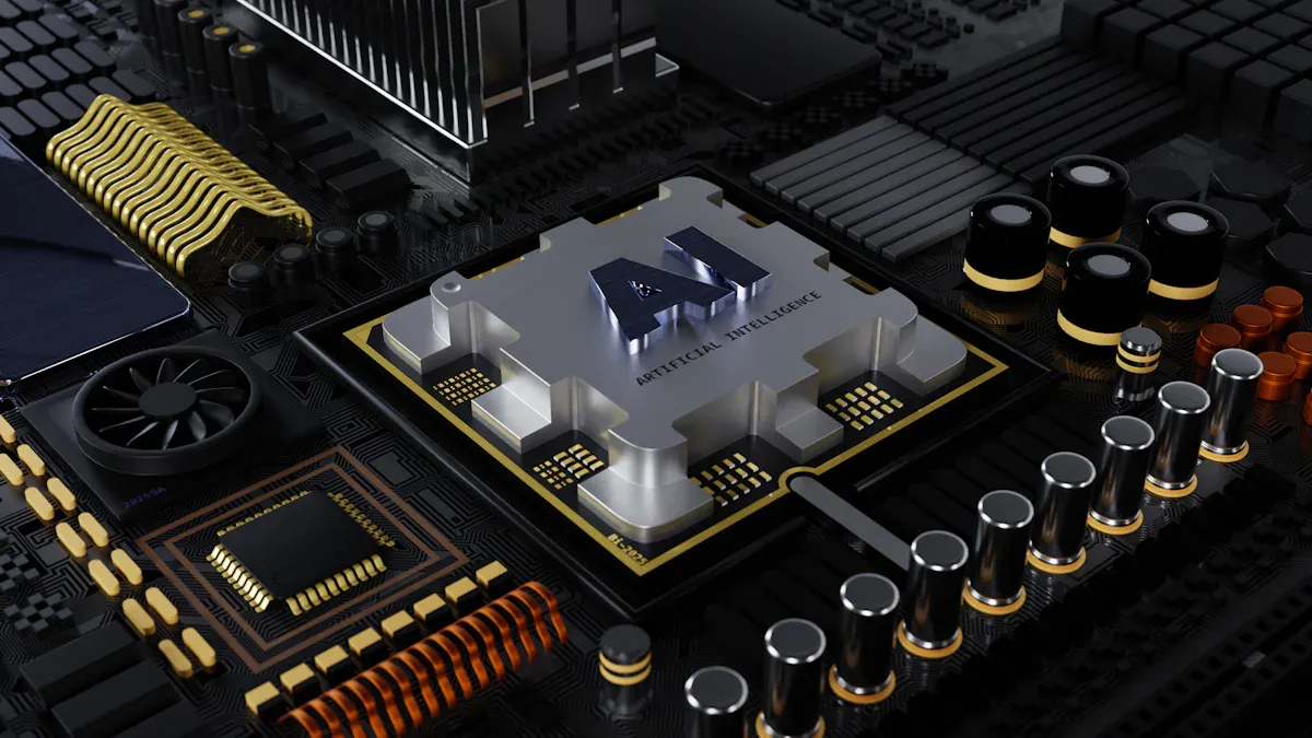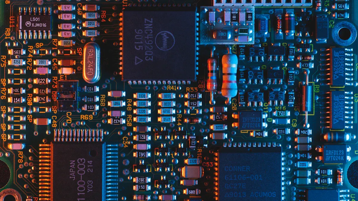
Designing high-speed PCBs for AI inference is crucial in today’s technology landscape. AI systems demand exceptional performance and reliable infrastructure to operate effectively. These systems process vast amounts of data and rely on high-speed PCBs for AI inference to ensure rapid signal transmission and stable power delivery. Memory speed plays a pivotal role in this process. For instance, AI often requires 300-700GB/s, and GDDR7 can deliver up to 192GB/s per device, enabling more compact and efficient AI designs.
However, developing high-speed PCBs for AI inference is a challenging task. Engineers must manage fast data rates, maintain signal integrity, and ensure sufficient power supply. Addressing these challenges is essential for optimizing the performance of AI systems.
Key Takeaways
Handle fast data by controlling impedance and using paired wires. This keeps signals clear and lowers interference.
Create good power systems to save energy. Add capacitors to steady power and make the PCB work better.
Keep signals strong with careful PCB design. Use tricks like the 3W rule and shields to protect signals.
Manage heat well with smart methods. Add heat sinks and special holes to cool down AI systems.
Pick the right parts and place them smartly on the PCB. This avoids delays and controls heat, improving performance.
Challenges in High-Speed PCB Design for AI Inference

Managing high data rates
High-speed PCBs for AI need to move lots of data fast. AI systems often handle data at speeds over hundreds of gigabytes per second. To keep signals clear, impedance control and signal quality are very important. Mistakes like using old design methods or skipping proper terminations can cause big problems.
To handle fast data rates well, focus on controlling impedance and reducing signal reflections. Using differential pair routing helps block noise and keeps signals timed correctly. Spacing traces with the 3W rule lowers crosstalk between signals. Stopping electromagnetic interference (EMI) is also key. EMI can mess up data transfer and weaken signals, so adding grounded guard traces or shielding lines helps a lot.
By following these steps, you can make high-speed PCBs work better for AI systems. This ensures fast and reliable data movement for powerful computing.
Addressing power demands
AI systems use a lot of power because they need to compute quickly. Regular hardware like CPUs and GPUs often waste energy. For example, getting data from external DRAM uses more energy than local registers. This affects how well the PCB performs overall.
To fix this, design power networks that lose less energy. Decoupling capacitors help keep power steady and reduce noise. For AI systems, balancing good power flow with saving energy is very important. New servers might use up to 1,000 watts by 2025, so planning for power needs is critical.
By focusing on power management, you can improve how high-speed PCBs work for AI tasks. This helps meet the needs of modern technology.
Ensuring signal integrity
Signal integrity means keeping signals strong and clear in high-speed PCBs. Without good design, signals can weaken, lose timing, or face interference. To protect signal quality, you need smart PCB layouts and routing plans.
Good methods include spacing traces with the 3W rule, using differential pair routing, and designing vias to avoid signal loss. Matching signal timing and length keeps everything in sync. EMI shielding, like grounding layers, cuts down on interference. Simulation tools let you find and fix signal problems before making the PCB, saving time and effort.
By using these ideas, you can keep signals steady and reliable. This is very important for AI systems and high-speed computing.
Power Management in High-Speed PCB Design
Efficient power delivery networks
Good power delivery networks (PDNs) are key for fast PCBs. Modern AI systems use chips needing low voltage and high current, often over 100 amps. These chips work at very high speeds, making power delivery tricky. You must design PDNs to handle these needs while staying stable and reliable.
To do this, lower impedance in the power path. Use wide traces and planes to cut resistance and inductance. Add extra ground layers to help current flow and reduce noise. Splitting power planes into sections can also make PDNs work better.
Studies show that advanced PDNs are vital for fast PCBs. As chips get stronger, they need better systems for steady power. By improving PDNs, you can boost how well high-speed PCBs work for AI inference.
Minimizing power losses
Cutting power waste is very important for AI inference systems. Fast PCBs often lose energy during data work and transfer. Fix this by improving power flow and cutting waste.
One way is to use special materials for PCB bases. These materials save energy and work more efficiently. Also, using power-saving tricks like changing voltage levels can lower energy use.
Tests show the value of saving power. For example, using 30% less power makes AI faster and models smaller. These changes make AI systems better for tough tasks.
Metric | Improvement |
|---|---|
Latency Reduction | 50% faster inference time |
Power Consumption | |
Model Size Reduction | 75% smaller models |
Decoupling capacitor strategies
Decoupling capacitors help keep power steady and cut noise in fast PCBs. They filter voltage changes and give smooth power to key parts.
To make them work best, use capacitors with different values. This spreads impedance evenly across many frequencies and lowers risks. Place capacitors close to power pins to reduce unwanted effects and improve performance.
Fast systems like CPUs and memory get big benefits from good capacitor setups. They see better signals and less noise, making them work reliably.
Use of Multiple Capacitors: Use capacitors with various values for wide frequency coverage.
Placement Strategies: Put capacitors near power pins to lower unwanted effects.
High-Speed Systems Examples: CPUs and memory work better with good capacitor setups.
By using these tips, you can keep power steady and make fast PCBs more reliable for AI inference.
Thermal Management for AI Inference Applications

Heat dissipation techniques
Managing heat is very important for AI systems. Overheating can harm parts and slow performance. To handle heat, spread it across the PCB or move it away from key parts. Copper layers and thermal pads spread heat sideways. Fans and heat sinks remove heat from the system.
Thermal analysis helps improve these methods. It finds hot spots and checks how well cooling parts work. For example, thermal maps show hot areas near power-heavy parts. This helps you place fans or heat sinks in the right spots. Planning for heat control early makes AI systems more reliable and avoids heat problems.
Using thermal vias and heat sinks
Thermal vias and heat sinks are great for cooling small PCBs. Thermal vias move heat from the surface to other layers or the back of the PCB. Groups of thermal vias with copper layers spread heat better and stop overheating.
Heat sinks work with thermal vias to cool parts. They take heat from parts and release it into the air. This is very useful for AI systems, which often get very hot in small spaces. Keeping parts cool helps them last longer and work better.
Thermal simulation tools
Thermal simulation tools are helpful for planning cooling systems. These tools let you test how heat moves on your PCB before making it. For example, ANSYS showed how simulations improved part placement in a car’s control unit, making it more reliable.
Simulations also test cooling ideas for factories. They show how heat spreads and how cooling parts work. Using these tools helps you fix problems early, save money, and keep AI systems running well under tough conditions.
Signal Integrity in High-Speed PCB Design
PCB stackup optimization
Improving the PCB stackup is key to keeping signals clear. A good stackup reduces interference and ensures reliable AI performance. Focus on these three important points:
Impedance control: Measure and manage trace impedances carefully. This stops signal reflections and keeps signals strong.
Return path management: Make sure signals have clear return paths. This lowers noise and keeps signals steady.
Layer pairing: Match signal layers with nearby ground planes. This improves signal quality and cuts down on EMI.
For example, a four-layer PCB with signal layers between ground and power planes works better than a two-layer PCB. Planning the stackup well helps create a strong system for high-speed AI PCBs.
Routing strategies for high-speed signals
Good routing is important for keeping signals strong in fast PCBs. Bad routing can cause crosstalk, EMI, and signal loss, hurting AI performance. Use these tips to avoid problems:
Space traces properly to lower interference.
Use ground planes to give return currents a clear path.
Keep traces short and direct to avoid delays.
Avoid sharp turns in traces; use smooth curves instead.
Limit the use of vias to prevent signal loss.
Advanced methods like differential pair routing and length matching help even more. Differential pair routing reduces noise by keeping paired signals together. Length matching ensures signals arrive at the same time, avoiding timing issues. These strategies help design PCBs that handle fast signals for AI tasks.
Signal integrity testing methods
Testing is very important to make sure your PCB works well. Without testing, your PCB might fail in real use. Try these testing methods:
Time-domain reflectometry (TDR): Use TDR to find impedance problems and signal reflections. Fixing these issues improves the PCB’s performance.
Eye diagram analysis: Create eye diagrams to check signal quality. A clear eye pattern means good signals, while a closed eye shows problems.
Simulation tools: Use simulation tools to predict signal behavior. For example, Artificial Neural Networks (ANNs) in simulations save time and reduce testing needs.
By using these tests, you can make sure your PCB meets AI system needs. Testing finds problems early and improves your design, making it more reliable and efficient.
Component Selection and Layout Optimization
Picking parts for fast AI systems
Choosing the right parts is very important for making fast PCBs for AI. Every part affects how well your design works. For AI, pick parts that handle fast computing and collect data accurately. These features are needed to manage AI’s heavy tasks.
Think about heat when picking parts. Hot parts can cause problems like broken solder or overheating. Choose parts that stay cooler or spread heat better. Testing parts early can help you find the best ones quickly. This makes it easier to adjust your PCB design.
Keeping signals clear is also important. Use parts with good trace designs, shielding, and terminations. These features help your PCB handle lots of data without losing signal quality. This builds a strong base for AI systems.
Placing important parts smartly
Where you put parts on the PCB matters a lot. Start by placing key parts, like processors and memory, close together. This shortens traces and reduces signal delays. Use multi-layer PCBs to save space and block interference.
Spread out hot parts to stop heat from building up in one spot. For example, don’t group power regulators and high-current parts together. Spread them out to keep the PCB cooler. Tools like CAD and thermal software can show how heat moves. These tools help you plan better and avoid costly fixes later.
Plan | What It Does |
|---|---|
Part Placement | |
Layer Use | Multi-layer PCBs save space and block interference. |
Heat Spread | Spreading hot parts stops heat from building up in one area. |
Simulation Tools | CAD and thermal tools help predict heat and improve designs. |
Routing and cutting parasitics
Good routing is key to stopping parasitic problems in fast PCBs. Parasitics, like unwanted inductance and capacitance, can mess up signals. As signals get faster, parasitic inductance gets worse. To fix this, lower inductance in your design.
Keep traces short and straight to avoid parasitics. Don’t use sharp angles, as they can cause signal issues. Add ground planes to give signals a clear return path. This lowers noise and crosstalk. Pairing traces closely (differential routing) also blocks noise and keeps signals clear.
Try to use fewer vias, as they can add unwanted capacitance. If you need vias, design them carefully to reduce their effects. These routing tips help keep signals strong and make your PCB work better for AI tasks.
Making a fast PCB for AI needs good planning and work. Focus on power, heat, and signal quality to keep it reliable. Use methods like better PCB layers, strong power systems, and smart cooling ideas. These steps help meet AI’s tough needs.
Use tools to find problems early and improve designs. Test carefully to fix issues before using the PCB. Change your design based on test results to make it work well. By doing these things, you can build strong PCBs for fast AI systems.
FAQ
What matters most in designing fast PCBs for AI?
Keeping signals clear is key. Make sure signals stay strong by improving PCB layers, routing paths, and impedance. Weak signals can cause errors and slow down performance.
How can you stop EMI in fast PCBs?
Use paired signal routing and grounded guard lines. These methods block noise and stop interference. Adding shield layers also protects signals from outside noise.
Why do AI systems need good cooling?
AI systems use lots of power, which makes them hot. Without cooling, parts can overheat and stop working well. Use heat vias, heat sinks, and testing tools to control heat.
How do decoupling capacitors help PCBs work better?
Decoupling capacitors keep power steady by filtering voltage changes. Place them close to power pins to cut noise and help fast parts like processors and memory run smoothly.
What tools check signal quality?
Tools like SPICE and TDR are very helpful. They find problems like signal mismatches or reflections before you build your PCB.
See Also
Streamlined PCBA Solutions for Your Electronics Projects
Best Practices for Maximizing Quality and Efficiency in PCBA
Enhancing Workflow Efficiency in PCB Assembly Processes
