Learning PCB and PCBA terms, including the PCBA acronym, is important in electronics. The global PCB and PCBA market is growing fast. It is expected to rise from $68.4 billion in 2023 to $105.8 billion by 2032. This growth shows how electronics are needed in many industries. Asia Pacific leads with over 50% of the market share.
Good communication is key in PCB projects. Knowing the right PCBA term, including the PCBA acronym, helps teamwork and avoids mistakes. Whether you design or build, this shared language makes work easier and faster.
People in OEM and electronics manufacturing use these terms often. Knowing them well, including the PCBA acronym, helps you work better and more accurately.
Key Takeaways
Knowing PCB and PCBA words helps teams talk clearly. Clear talk makes teamwork easier and better.
Learning acronyms like BOM and DFM makes design faster. It also helps avoid mistakes and saves time.
Using the right words helps you read guides and plans. This skill makes you better at electronics.
Learning terms like Gerber files and reflow soldering helps make good PCBs. These words help finish projects well.
Using PCB and PCBA words right improves project results. It means fewer mistakes and better success rates.
Understanding PCB and PCBA Terminology
What is a Printed Circuit Board (PCB)?
A printed circuit board is the base of modern electronics. It links parts using thin paths called traces. These traces are made on copper layers, separated by insulating materials. The board is layered and gives support while connecting parts.
PCBs are important for making electronics quickly and cheaply. They help place parts exactly where needed, speeding up production. Almost all devices, like phones and machines, need PCBs to work. With advanced chips, PCBs allow fast data transfer and communication.
Main parts of a PCB include vias, which link layers, and pads, which attach parts. This design makes sure the board works well and lasts long, meeting electrical and heat needs.
What is a Printed Circuit Board Assembly (PCBA)?
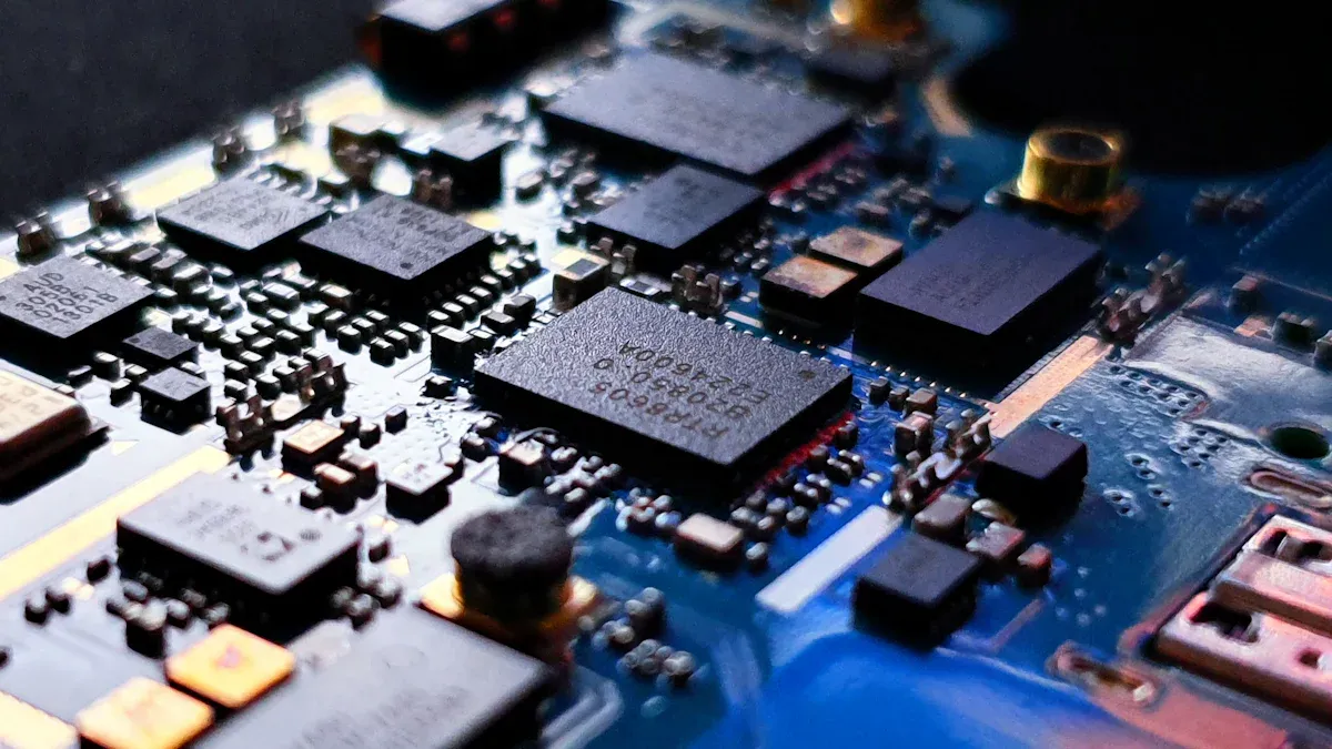
A printed circuit board assembly means adding parts to a bare board. This turns the board into a working unit that does specific jobs. Parts like resistors and chips are placed on the board by machines.
The process has steps like adding solder paste, placing parts, and heating to stick them. Advanced methods make sure parts are placed right and stay connected. After assembly, testing checks if everything works properly.
PCBA is very important in making electronics. It helps meet the need for devices like smart gadgets and phones. By combining design and assembly, PCBA makes high-quality electronics for many uses.
Why is terminology crucial in the PCB industry?
Knowing PCB terms helps you talk clearly with others. Words like “trace,” “via,” and “core” explain parts of a circuit. Learning these words makes it easier to discuss designs and production.
Using the right terms helps teams work together better. Engineers and builders use the same words to avoid mistakes. This saves time and reduces errors during production.
Also, knowing these terms helps you understand technical guides. Glossaries and definitions explain PCB and PCBA processes. Learning this language improves your skills in electronics work.
Key PCBA Acronyms and Their Meanings
Knowing the acronyms in the PCB and PCBA field is important. These short forms make hard ideas easier to understand. They help you work better in electronics. Below are some common acronyms used in designing, making, and testing PCBs.
Common PCB Acronyms (e.g., PCB, PCBA, SMT, SMD)
PCB (Printed Circuit Board): This is the base board in electronics. It links parts with conductive paths to make circuits work.
PCBA (Printed Circuit Board Assembly): This is when parts are added to a PCB to make it work.
SMT (Surface Mount Technology): A way to place parts directly on a PCB‘s surface. It allows smaller designs and faster production.
SMD (Surface Mount Device): These are the parts used in SMT, like resistors and chips.
These acronyms explain how parts are placed and connected on a board. They are key to understanding PCB and PCBA basics.
Manufacturing Acronyms (e.g., BOM, DFM, DRC)
BOM (Bill of Materials): A list of all parts needed to build a PCB. It includes details like part numbers and quantities.
DFM (Design for Manufacturing): This makes sure a PCB design is easy and cheap to produce. It spots problems early in the design.
DRC (Design Rule Check): A check to see if a PCB design follows manufacturing rules. It helps avoid production mistakes.
These acronyms help make the manufacturing process smoother. They prevent errors and ensure high-quality boards.
Testing and Quality Acronyms (e.g., ICT, AOI, ESD)
ICT (In-Circuit Test): A test to check if each part on a PCB works properly.
AOI (Automated Optical Inspection): A camera-based check to find defects like bad soldering or misplaced parts.
ESD (Electrostatic Discharge): Sudden electricity flow that can harm PCB parts. Protecting against ESD is very important.
Testing ensures PCBs are reliable and meet standards. It lowers costs and improves customer trust. The table below shows why testing matters:
Performance Metric | Importance |
|---|---|
Finds and fixes problems that could make PCBs fail. | |
Reducing costs | Catches issues early, saving money on repairs or rework. |
Meeting regulatory requirements | Confirms the board meets rules, avoiding fines or legal trouble. |
Improving customer satisfaction | Makes sure products work well, keeping customers happy. |
Learning these acronyms helps you understand testing and quality checks. This knowledge ensures you create reliable PCBs.
Important Words in PCB Design and Making
Design Words (e.g., Gerber Files, Via, Trace)
Knowing design words helps make a good and working PCB. These words explain how the board is built and how parts connect.
Gerber Files: These files are like maps for your PCB. They show the layout of each layer, including copper paths, solder masks, and labels. Factories use these files to make the board correctly. They include details like drill spots and sizes to match the design plan.
Trace Routing: Traces are tiny paths that carry signals between parts. Good routing keeps signals clear. Tips include keeping paths smooth and avoiding extra bends, especially for fast circuits.
Via Placement: Vias are tiny holes that link layers of the board. Placing them well stops signal problems and makes the board work better. Special vias, like blind or buried ones, save space in tricky designs.
A good PCB needs these design words. For example, Gerber files help make the board right, while good trace routing and via placement improve how it works.
Design Word | How It Helps |
|---|---|
Gerber Files | Needed for making the board, showing each layer’s layout. |
Trace Routing | Tips include smooth paths and avoiding extra bends for clear signals. |
Via Placement | Placing vias well stops signal issues and saves space in complex designs. |
Making Words (e.g., Substrate, Solder Mask, Silkscreen)
Making words are key to building strong and lasting PCBs.
Substrate: This is the board’s base, often made of fiberglass. It holds the circuit and keeps it safe from electricity.
Solder Mask: This layer covers copper paths to stop rust and solder mistakes. It helps the board last longer and work better.
Silkscreen: This layer adds labels and marks to the board. It helps workers put parts in the right spots and fix problems easily.
Making Word | How It Helps | What It Does |
|---|---|---|
Solder Mask | Protects copper paths | Stops rust and solder mistakes, making the board last longer. |
Silkscreen | Adds labels | Shows part names and guides workers during building and fixing. |
Using good materials like substrates, solder masks, and silkscreens makes sure your PCB works well and meets industry rules.
Assembly Words (e.g., Reflow Soldering, Pick-and-Place, Stencil)
Assembly words explain how to turn a plain PCB into a working PCBA. These steps are important for making high-quality boards.
Reflow Soldering: Heat melts solder paste to stick parts to the board. This makes strong connections and is common in factories.
Pick-and-Place: Machines carefully put parts on the board. This step is important for speed and accuracy in big projects.
Stencil: A stencil spreads solder paste on the board before adding parts. It makes sure paste goes only where needed, saving time and materials.
Metric | What It Means |
|---|---|
Counts mistakes per million chances, helping compare quality. | |
First Pass Yield (FPY) | Shows how many boards pass checks the first time, showing process success. |
Rework Rate | Tells how many boards need fixing after assembly, with fewer fixes meaning better quality. |
Scrap Rate | Counts boards that can’t be used due to mistakes, with fewer scraps boosting productivity. |
Good assembly steps, like reflow soldering and pick-and-place, lower mistakes and make better PCBAs.
Real-World Uses of PCB and PCBA Words
How Acronyms and Words Help in PCB Design
Knowing PCB acronyms and words helps make better boards. Words like BOM, Gerber files, and schematics are very important. A BOM lists all parts needed for the board. It helps plan costs and order items easily. Gerber files are like maps that guide factories to build boards correctly. Schematics show how parts connect, helping avoid mistakes.
Tools like Altium Designer, Eagle PCB, and KiCAD use these words. These tools help you draw schematics, make Gerber files, and handle BOMs. Learning these terms helps you use design tools better and work faster.
Why Words Matter in Manufacturing
In factories, words make work clear and smooth. Words like substrate, solder mask, and silkscreen explain board parts. Substrate is the board’s base. Solder mask protects copper paths during assembly. Silkscreen adds labels to help with building and fixing.
Terms like DFM and DRC improve manufacturing. DFM makes boards easier to build. DRC finds mistakes before making the board. These steps save time and improve quality. For example, a telecom company used these terms to make complex boards for their needs.
Working Together with Shared Words
Using the same words helps teams work well together. It avoids confusion and costly errors. For example, a car company needed special PCBAs for safety. Clear words about rules and steps helped meet strict standards.
Another example is a startup making electronics. They had trouble growing because of unclear plans. By agreeing on words like prototyping and scaling, they fixed their process. Whether for IoT or medical devices, knowing PCB words helps teamwork and success.
Knowing PCB and PCBA words is very important in electronics. It helps you talk clearly, avoid mistakes, and finish projects faster. Words like trace, solder mask, and Gerber files help you design and build boards that work well.
This blog can help you learn and feel more confident. Using clear words makes teamwork better and gives great results. For example, good use of terms often leads to a first pass yield of 95% to 98%. Mistakes per million chances drop to 500 to 1000. Customer returns also go below 1%, as shown here:
Metric | Value Range |
|---|---|
First Pass Yield (FPY) | 95% to 98% |
Defects Per Million Opportunities (DPMO) | 500 to 1000 |
Customer Return Rate | Less than 1% |
Learning these words improves board quality, saves time, and makes customers happy. Focus on using the right words to succeed in your projects.
FAQ
1. What is the difference between PCB and PCBA?
A PCB is just the plain board with paths for electricity. A PCBA has all the parts added to the PCB. The PCBA is ready to be tested or used in devices.
2. Why are Gerber files important in PCB manufacturing?
Gerber files are like maps for making a PCB. They show how to build each layer, including paths, masks, and labels. Without them, mistakes can happen during production.
3. What does SMT mean in PCB assembly?
SMT means Surface Mount Technology. It’s a way to attach parts directly to the board’s surface. This method makes designs smaller, faster, and more efficient.
4. How does AOI improve PCB quality?
AOI (Automated Optical Inspection) uses cameras to find problems like misplaced parts or bad soldering. It helps make better boards by catching mistakes early.
5. Why is ESD protection crucial in PCB assembly?
Electrostatic discharge (ESD) can harm delicate parts on a PCB. Using ESD protection, like grounding or special materials, stops damage and keeps the board working well.
💡 Tip: Always handle PCBs in a safe area to avoid damage from static electricity.
See Also
Exploring PCBA: Definition And Its Importance In Electronics
Defining PCBA And Its Significance In Electronic Systems
The Role Of PCBA In Defining Electronic Devices