What will change manufacturing PCB in 2025? Engineers are spotting new trends in PCB technology that are set to transform the manufacturing PCB process. These include HDI, flexible PCBs, and embedded parts, all driving rapid change. Understanding these innovations helps teams create better designs, enhance functionality, and promote environmental responsibility. New manufacturing PCB methods incorporate automation, AI, and eco-friendly materials, enabling companies to meet quality and sustainability goals. Embracing these trends gives businesses a significant competitive advantage.
HDI and miniaturization for small devices
Flexible and rigid-flex PCBs for wearable tech
Advanced materials for high-frequency uses
AI and automation for smarter manufacturing PCB processes
Key Takeaways
New PCB technologies like HDI, flexible PCBs, and embedded parts help make devices smaller. These devices are smarter and more reliable.
Automation and AI make PCB manufacturing faster. They help reduce mistakes and save money.
Advanced materials like Rogers and Teflon laminates improve signal quality. This is important for high-frequency uses like 5G and radar.
Sustainable PCB designs use eco-friendly materials. Green manufacturing helps protect the environment and lowers costs.
Cloud tools and IoT integration help teams work together better. They allow real-time monitoring and smarter production in PCB manufacturing.
Top Trends in PCB Manufacturing
The biggest trends in pcb manufacturing for 2025 show fast changes in technology and what customers want. Companies are now working on high-density designs, flexible and stretchable pcbs, and using more automation in pcb manufacturing. These new ideas in pcb technology help make better devices and support the environment. Engineers and manufacturers get many benefits from these new solutions. They can make products that are smaller, smarter, and more reliable.
Key Trends Shaping PCB Manufacturing in 2025:
High-Density Interconnect (HDI) PCBs
Flexible and Rigid-Flex PCBs
Advanced materials for high-frequency applications
Smart PCBs with integration of AI and IoT
HDI & Miniaturization
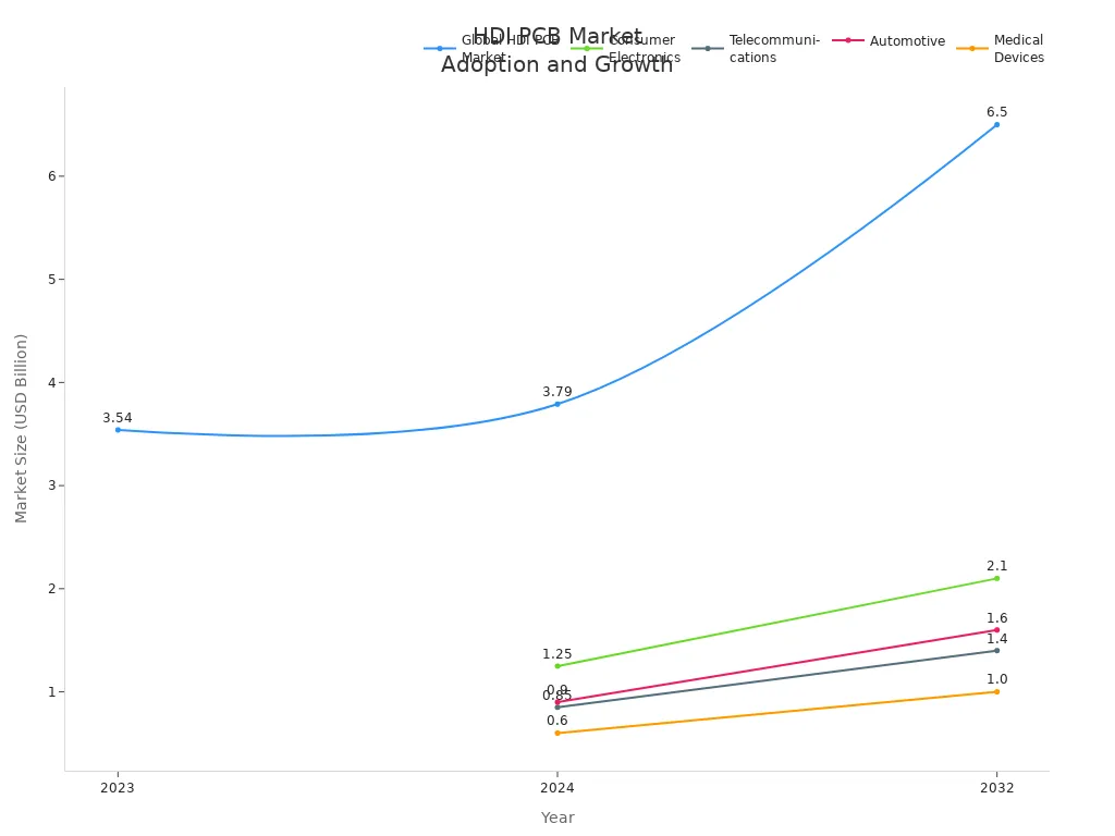
High-density circuits and miniaturization lead the way in pcb manufacturing. HDI PCBs use microvias, blind and buried vias, and thin lines to fit more connections in less space. This lets companies make tiny pcbs for electronics, cars, and medical tools. The worldwide HDI PCB market could grow from $12.5 billion in 2023 to $23.8 billion by 2032, with a CAGR of 7.1%. This shows how miniaturization and flexible circuits are needed in many fields.
Metric/Segment | 2023 (USD Billion) | 2024 (USD Billion) | 2032 Projection (USD Billion) | CAGR (2025-2032) |
|---|---|---|---|---|
Global HDI PCB Market | 3.54 | 3.79 | 6.5 | ~6.99% |
Consumer Electronics | N/A | 1.25 | 2.1 | N/A |
Telecommunications | N/A | 0.85 | 1.4 | N/A |
Automotive | N/A | 0.9 | 1.6 | N/A |
Medical Devices | N/A | 0.6 | 1.0 | N/A |
North America Market | N/A | N/A | 2.0 | N/A |
APAC Market | N/A | 1.75 | N/A | N/A |
Manufacturers use microvia technology to make vias as tiny as 0.1 mm. This helps fit more parts on the board and saves space. HDI PCBs can make boards up to 60% smaller, so devices are thinner and lighter. These boards help with fast connections for 5G and Wi-Fi 6, making signals better and keeping things cool. Automated design tools help engineers be exact and reliable, even with complex high-density designs.
Flexible & Rigid-Flex PCBs
Flexible and rigid-flex pcbs give designers many choices for new electronics. Flexible pcbs can bend and twist, so they work well in wearables, phones, and medical tools. Rigid-flex pcbs mix the strength of hard boards with the flexibility of soft circuits, so they last longer in tough places like cars and planes.
Flexible and stretchable pcbs help make small, light products that fit in tight spaces.
These boards can handle shaking and bending over and over, so products last longer.
Rigid-flex pcbs need fewer connectors and solder joints, so they break less and work better.
Flexible pcbs make building things easier, cost less, and lower mistakes.
Better heat control and steady electrical features make flexible and rigid-flex pcbs good for powerful devices.
Designers use flexible pcbs to make tricky, 3D layouts. This helps create cool products that people want because they are easy to carry and strong. The trend of making things smaller and using flexible circuits is growing, especially in health, space, and IoT.
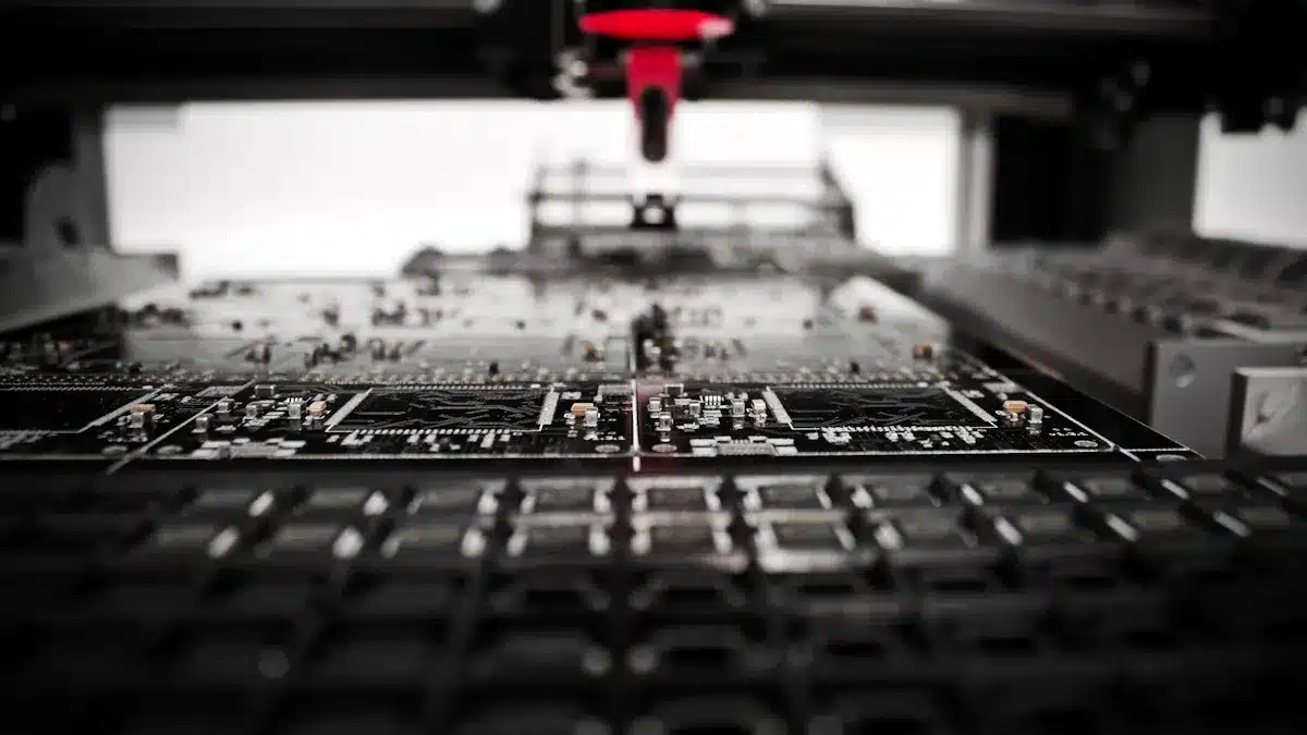
Automation & AI
Automation in pcb manufacturing and AI-powered design tools are changing how things are made. AI tools help with drawing schematics, picking parts, and routing, so designs are finished faster. Automated inspection finds problems early, so quality is better and less is wasted. Machine learning helps plan production and use resources better, which saves money and time.
Automated material handling and inventory keep parts in the right place.
Robots work with people, mixing accuracy and creativity.
AI helps fix machines before they break, so there is less downtime.
Watching and improving the process in real time keeps quality high.
Siemens used causal AI at their Erlangen plant and cut PCB defects below the Six Sigma level. This saved money and improved results. The investment paid off in just one year, showing how helpful AI and automation are in pcb manufacturing. Companies using these tools finish jobs faster, work better, and make more reliable products.
Advanced Materials for High-Frequency Applications
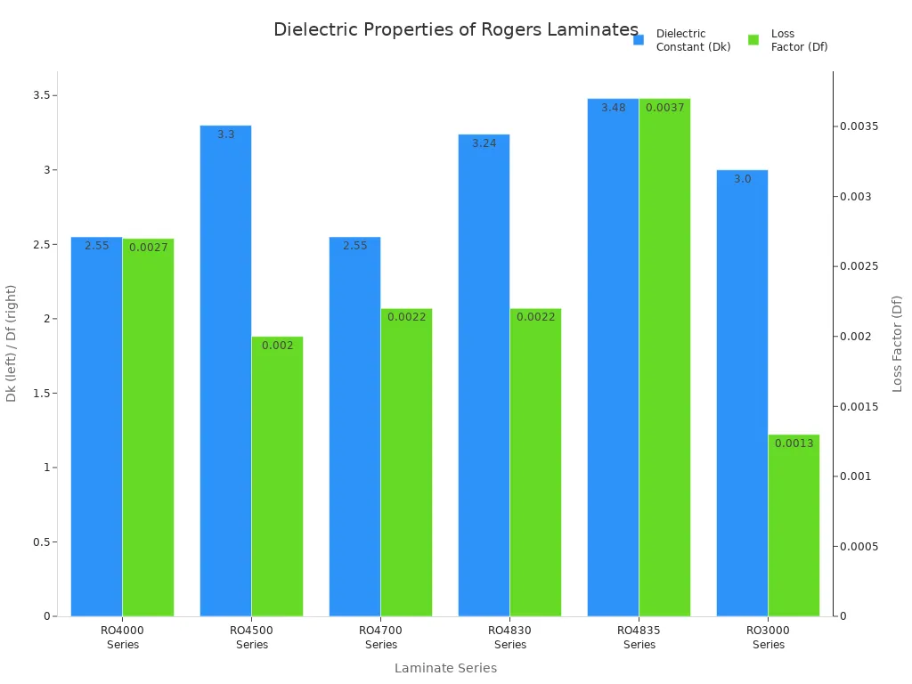
Rogers & Teflon Laminates
Engineers pick Rogers and Teflon laminates for high-frequency designs. Rogers laminates, like RO4000 and RO3000, have stable dielectric constants and low loss. These features help keep signals strong in microwave and millimeter-wave circuits. Teflon, also called PTFE, has a very low dielectric constant and dissipation factor. This makes it great for RF and microwave circuits. PTFE is often made stronger with glass fiber. Rogers laminates work well with normal PCB manufacturing steps. PTFE-based materials sometimes need special handling.
Laminates Series | Dielectric Constant (Dk) | Loss Factor (Df) | Processing Compatibility | Mechanical & Thermal Properties | Performance Highlights |
|---|---|---|---|---|---|
RO4000 Series | 2.55 – 6.15 | ~0.0027 – 0.0038 | Standard FR-4 | Low CTE, flame retardant | Low loss, stable Dk |
RO3000 Series | As low as 0.0013 | Special PTFE processing | Low CTE, stable Dk | Lowest loss, RF/microwave | |
PTFE (Teflon) | 2.1 – 2.5 | 0.0002 – 0.0004 | Special processing | Excellent thermal stability | Ideal for RF/microwave |
Material Benefits
Advanced materials for high-frequency uses are better than standard FR-4. They have low dielectric constants and dissipation factors. This means less signal loss and better signal quality. Rogers and PTFE-based laminates work at frequencies above 10 GHz. They are good for radar, satellite, and 5G systems. Their strong thermal stability helps devices handle lots of power without getting too hot. Some new materials, like graphene and nanodiamond-based thermal interface materials, move heat even better. This keeps devices cool and working well. Engineers also use insulated metal PCBs to control heat and protect signals.
Tip: Picking the right material makes devices work better and last longer, especially in tough places.
Selection Challenges
Choosing advanced materials is not always easy:
Engineers look for materials with low dielectric loss and steady impedance.
Making PCBs with PTFE or ceramic-filled laminates can be hard because of sticking and processing needs.
Small changes in trace width or thickness can change how the board works, so tight tolerances are needed.
Signal problems like crosstalk and electromagnetic interference need careful planning.
Working with PCB suppliers helps balance performance, price, and how easy it is to make.
Engineers must think about all these things to get the best results for high-frequency designs.
Manufacturing PCB with 3D Printing

Conductive Inks
Engineers use special conductive inks for 3d-printed electronics. These inks help make prototypes quickly and let people change designs easily. Nano-particle inks conduct electricity well and dry fast, so they work for speedy jobs. Graphene inks bend easily and carry electricity well, so they fit wearable devices and curved boards. PEDOT:PSS inks are very good for 3d-printed electronics. They can reach up to 155 S cm⁻¹ when dry and 28 S cm⁻¹ in hydrogel form.
Conductive Ink Type | Conductivity (Dry State) | Conductivity (Hydrogel State) |
|---|---|---|
PEDOT:PSS-based conducting polymer ink | Up to 155 S cm⁻¹ | Up to 28 S cm⁻¹ |
Silver nanoparticle inks conduct electricity very well but cost more. Copper inks are cheaper but can rust. Engineers also try using ceramic inks for special jobs. These materials let people print tiny details as small as 20 microns. This helps build complex multilayer PCB designs.
Tip: Picking the best ink makes signals better and devices work well, especially for high-frequency circuits.
Additive Techniques
Additive manufacturing has changed how teams make 3d-printed electronics. Inkjet printing puts down inks very accurately, so tiny features and many layers are possible. Aerosol jet printing uses a thin stream to make tricky shapes and works on curved surfaces. Fused Deposition Modeling (FDM) pushes out plastic for insulation, then adds conductive lines, so many layers can be built. Direct Ink Writing (DIW) squeezes thick inks to make tall 3D shapes.
Additive Manufacturing Technique | Description and Role in PCB Fabrication |
|---|---|
Inkjet Printing | Puts down conductive and insulating inks very precisely, making tiny features and many layers. |
Aerosol Jet Printing | Uses a thin stream to place materials, making tiny details and tricky shapes. |
Fused Deposition Modeling (FDM) | Pushes out plastic to make insulation; adds conductive lines later, so many layers are possible. |
Direct Ink Writing (DIW) | Squeezes thick inks to build tall 3D shapes, making complex circuit designs. |
These methods let engineers make custom shapes, curved PCBs, and put parts inside boards. Antennas, coils, and capacitors can go right into the board, which was hard before. New tools like high-resolution extruders and smart software make printing better and more exact. Easy-to-use design programs and cheaper printers help more people try 3d-printed electronics, so new ideas grow in many fields.
mSAP & Panelization
Finer Features
mSAP is a new way to make tiny features on printed circuit boards. It uses a special copper process and very accurate lithography. Engineers can now make lines and spaces smaller than 10μm, sometimes as small as 3μm. This helps build high-density layouts for advanced electronics. The process starts with a thin copper layer. Then, photoresist is added and patterned. Next, copper is put on only where it is needed. The base copper is removed at the end. This leaves a board with very exact lines and little change in size.
Aspect | mSAP (Modified Semi-Additive Process) | Traditional Subtractive Process |
|---|---|---|
Minimum Line Width/Spacing | Below 10μm, down to 3μm | Typically 20μm |
Line Geometry Control | Excellent, minimal variation | Prone to undercut and variation |
Material Usage | Efficient, copper only where needed | Wasteful, up to 70% copper wasted |
Signal Integrity | Superior, consistent lines | Compromised at fine geometries |
mSAP lets engineers design small PCBs with tight spaces and many traces. This method also makes signals better by lowering crosstalk and keeping impedance steady. The process uses thinner layers, so boards are lighter and thinner. mSAP helps make small devices like smartphones and wearables with great accuracy.
Faster Builds
Panelization makes PCB production faster by putting many boards on one panel. This way, manufacturers can work on several boards at the same time. It saves time and cuts costs. Engineers use panelization to make work smoother and reduce mistakes. When used with mSAP, panelization helps build boards quickly and keeps quality high.
Panelization cuts down setup time for each board.
It lets machines check and test many boards together.
Finished boards can be separated fast with routing or lasers.
This method lowers waste and boosts the number of good boards made.
Note: Using mSAP and panelization together helps companies finish jobs on time and make products you can trust.
Embedded Components
System-in-Package
System-in-package technology changes how engineers make electronics. SiP puts many chips and modules in one small package. This lets digital, analog, and RF chips work together in one unit. Engineers use SiP for devices that need to be fast and tiny. SiP makes signal paths shorter. Shorter paths mean less signal loss and faster speed. Devices like smartphones and wearables use SiP for their cool features.
SiP has many good points:
It puts processors, memory, sensors, and RF modules in a small spot.
Different parts can work together, so devices do more things.
3D packaging and through-silicon vias help with speed and power.
Special packaging helps control heat, so devices last longer.
SiP helps companies make new products faster.
Engineers use SiP in cars to save space and meet tough rules. Chips made from different materials work together and do their jobs better. This helps with things like AI processors and 5G devices.
Space Saving
Putting parts inside PCB layers helps engineers save space. This makes products smaller. It can shrink board size by up to 40 percent. More space means more features or lighter designs. Shorter connections inside the board make signals better and faster. Devices work well and are more reliable.
Main benefits of embedded parts are:
Smaller devices and better use of space.
Better electrical performance with less interference.
More reliability because parts are safe from water and shaking.
Lower costs when making lots of boards.
Better heat control with copper blocks and thermal vias.
Designers use embedded parts in flexible and stretchable PCBs for tight spots. These ways help make strong devices for tough places. Engineers see fewer problems and less fixing needed. Embedded parts let people design light, smart electronics for many uses.
Sustainable PCB Designs
Green Manufacturing
Sustainable pcb designs are very important now. Companies want to help the planet. They use green manufacturing to make less waste and pollution. Many factories use lead-free soldering. They pick tin-silver-copper alloys to follow rules like RoHS. This change keeps workers and nature safe from lead. But mining silver and copper still causes problems. Recycling programs help get metals back and cut down on e-waste.
Factories also use halogen-free laminates. This lowers toxic smoke when boards are thrown away. Some companies clean and reuse water so it does not get dirty. Energy-saving ways like LED curing and solar power help use less energy. These steps lower carbon emissions. Automation and AI watch resources, cut waste, and make work better.
Companies that use green manufacturing save money. They make better products and customers trust them more.
Eco Materials
Eco-friendly materials help engineers make safer PCBs. Lead-free solder and halogen-free laminates are less toxic. They make recycling easier. Biodegradable pcb substrates use cellulose or natural fibers. These break down on their own and help the circular economy. Bio-based resins and recycled materials also lower harm to the planet.
Designers use modular layouts and less material. This makes taking apart and recycling easier. Additive manufacturing like 3D PCB printing uses only what is needed. This cuts waste. These new ideas follow world rules and meet what customers want.
Eco Material Type | Environmental Benefit |
|---|---|
Lead-free solder | Makes less dangerous waste |
Halogen-free laminates | Lowers bad smoke |
Biodegradable substrates | Break down in nature |
Recycled materials | Save resources, cut e-waste |
Focusing on sustainability pushes the industry to use new materials and smart ways. Companies that do this get more jobs and build a good name for caring about the planet.
Cloud & IoT in PCB Manufacturing

Cloud-Based Design Tools
Cloud-based design tools are changing how engineers make PCBs. These tools have many benefits.
Subscription plans cost less at the start, so small companies can use them.
Engineers do not need powerful computers because the software runs online.
Updates and fixes happen by themselves, so there is less waiting and fewer extra costs.
Companies can pay for more or fewer licenses as needed, which saves money.
Teams in different places can work together at the same time, so designs get done faster.
Built-in libraries and testing tools help engineers check parts and designs early, so they avoid big mistakes.
Cloud tools like Altium 365 and Cadence OrCAD X Symphony let many engineers work on one design together. This helps keep track of changes and lowers mistakes. All the data is in one place, so teams can make good choices and finish work quickly. But engineers need to think about internet problems and keeping data safe. Many companies now use strong encryption and let people work offline to help with these issues.
IoT Integration
IoT brings new ways to make PCBs better. Sensors inside the factory watch the process all the time. They find problems early and help make better boards. After products are made, sensors keep checking them. This helps fix things before they break and makes products last longer. Using data and machines cuts waste and makes things faster.
Watching in real time means less scrap.
Fixing things before they break makes devices last longer.
Machines that work by themselves save money and time.
New ways to build, like additive manufacturing and microvia technology, help IoT work well.
Power is still a problem because many IoT devices use batteries. Engineers need to pick parts that use less power and find ways to get energy from the environment. Keeping devices safe is also very important. Encryption and safe ways to talk keep devices safe from hackers. Making smart PCBs for IoT needs careful planning to fit wireless parts and sensors in small spaces. Teams also need to watch parts and schedules to stop delays.
Challenge | Description |
|---|---|
RF parts need careful design to stop losses and interference. | |
Compact integration | Putting many parts on small boards is hard and needs smart layouts. |
Manufacturability | Designs must match what factories can do. |
Supply chain management | Teams must watch parts and suppliers to stop running out. |
Production management | Planning assembly and tools changes how fast products are finished. |
New changes in pcb manufacturing help make things faster and greener.
Industry 4.0, additive manufacturing, and smart factories help build prototypes quickly and make things exact.
Robotics, AI, and eco-friendly materials help companies waste less and make better products.
Better supply chains and making things closer to home help save money and make products more reliable.
Learning about new trends helps companies create new ideas, meet what customers want, and earn trust.
What engineers and businesses should do next:
Try modular layouts and use better design tools.
Work with fast manufacturers and trusted recyclers.
Find helpful articles, online classes, and forums to keep learning.
Resource Category | Description |
|---|---|
Articles about DFM, stack-up, and IPC standards | |
Materials & Types | Guides on substrates, flex, rigid-flex, and advanced PCBs |
Advanced PCB Types | HDI PCB manufacturing and gold fingers |
Courses | Online classes for picking materials and learning about making PCBs |
Community & FAQs | Forums and FAQs for getting technical help |
FAQ
What is the main benefit of using HDI PCBs?
HDI PCBs let engineers put more connections in less space. This means devices can be smaller and lighter. These devices also work better. Medical and car companies use HDI for new products.
How do flexible PCBs improve product design?
Flexible PCBs can bend and twist to fit tight spots. Designers use them in wearables, phones, and medical tools. These boards last longer because they handle movement and shaking.
Why do engineers choose advanced materials for high-frequency PCBs?
Engineers pick materials like Rogers and Teflon for high-frequency PCBs. These materials help signals stay strong and clear. They are used in 5G, radar, and satellites.
How does automation help in PCB manufacturing?
Automation makes production faster and improves quality. Machines do jobs like checking boards and moving parts. This lowers mistakes, saves time, and cuts costs.
What role does the integration of ai and iot play in modern PCB manufacturing?
Adding ai and iot lets factories watch things in real time. Sensors and AI tools find problems early. They help use resources better and make products more reliable.
See Also
Emerging Innovations Shaping PCB And PCBA Design Processes
In-Depth Look At PCBA Testing Methods For Electronics
Benefits And Obstacles Of Flex PCBA In Electronics