You can find mobile pcba in almost every device today. Each mobile pcba type fits a different device need. It also changes how well your device works. PCBA means Printed Circuit Board Assembly. This is where electronic parts connect and talk to each other. It helps your phone or wearable device work. Picking the right pcba can make your device work better. It can also make it more reliable. The market for mobile pcba is getting bigger. More companies want better performance, smaller size, and new features like hdi design. The table below shows what is happening in the market:
Aspect | Details |
|---|---|
USD 27.5 billion | |
Projected Market Size 2032 | USD 44.9 billion |
CAGR (2023-2032) | 5.7% |
Flexible PCB Adoption | Growing due to foldable phones and wearables |
Key Market Drivers | 5G, miniaturization, multifunctional integration |
You should know the main types of pcba. You also need to know how they are different. Some give better performance for your device. Picking the right one helps you stay ahead. This is important as hdi technology and mobile apps keep changing.
Key Takeaways
Mobile PCBA links parts inside devices. It changes how well devices work. It also changes their size and how long they last.
There are different PCBA types for different uses. Single-layer PCBA is for simple devices. Multilayer and HDI PCBA are for small, fast, and advanced gadgets.
Flexible and rigid-flex PCBAs can bend and fold. They are great for wearables and foldable phones.
Picking the best PCBA means thinking about what the device needs. You must also think about materials, signal quality, and how it is made.
PCBA is tested with heat, shaking, and X-ray checks. This makes sure it is strong and does not break easily.
PCBA Overview
What Is PCBA
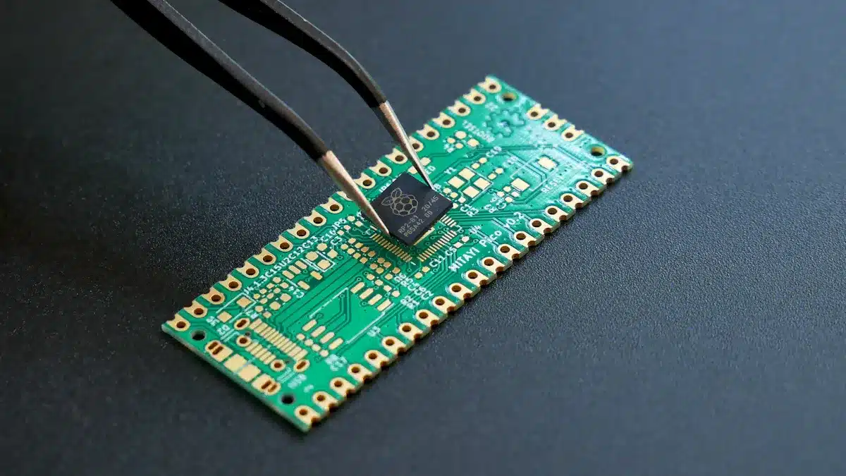
Have you ever thought about how your phone works? The answer is often the printed circuit board assembly, or PCBA. This is the main part inside every electronic device. A PCBA is a printed circuit board with parts like chips and resistors attached. The board is flat and made from things like fiberglass. It has thin metal lines that let electricity move around. When the parts are added and connected, it becomes a printed circuit board assembly.
The story of PCBA shows how much technology has changed. Roots Analysis says the market for printed circuit boards has grown since 2019. New materials, better designs, and smart machines made PCBA smaller and faster. These changes also made them more reliable. Wevolver says companies use advanced tools and quality checks, like X-ray inspection, to make sure each printed circuit board assembly works well. You can see these changes in devices like the Apple iPhone X and Fitbit Charge 4. These use advanced PCBA and hdi technology for better performance.
Role in Mobile Devices
You use your mobile device every day. The PCBA inside helps it work well. It connects the battery, screen, camera, and other parts. The design of the printed circuit board affects speed, battery life, and size. Engineers use special software to test the PCB. They check how it handles heat, power, and signals. This helps them find weak spots and make the design better.
Tip: Many tests, like stress and heat tests, help make sure your device will not break when you need it.
PCBA uses strong materials and smart design to handle drops, heat, and daily use.
Companies use special alloys and solder to help the printed circuit board assembly last longer.
Following strict industry rules, like IPC standards, keeps your device safe and reliable.
Modern devices need more from their PCBA. With hdi and flexible PCB, you get thinner phones and more features. The right design lets you enjoy fast, reliable, and powerful devices every day.
Mobile PCBA Types
Single-Layer PCBA
Single-layer PCBA is in simple devices. It has one copper layer on one side. The design is easy to make and test. You see it in things like calculators and remote controls. LED lights also use single-layer PCBA. These boards use FR-4 or aluminum. Aluminum helps with heat.
Here is a table that shows how single-layer and multi-layer PCBAs are different:
Aspect | Single-Layer PCB | Multi-Layer PCB |
|---|---|---|
Structure | One copper layer on one side of substrate | Multiple copper layers separated by insulating layers |
Complexity | Simple design, easy to manufacture | Complex design, supports intricate circuits |
Cost | Lower production cost | Higher cost due to multiple layers |
Performance | Good for low-power, low-speed applications | Handles high-speed signals, complex data processing |
Application Examples | Remote controls, LED lights | Smartphones, computers |
Size and Weight | Larger and heavier | More compact and lighter |
Heat Dissipation | Limited, better with aluminum-backed | Improved through internal layers |
Flexibility | Rigid or flexible for simple designs | Rigid-flex for compact, high-performance devices |
Note: Single-layer PCBA is best for simple and cheap devices. It is not good for hard circuits or fast signals.
Double-Sided PCBA
Double-sided PCBA has copper on both sides of the board. You can put parts on the top and bottom. This makes more complex circuits than single-layer boards. You find double-sided PCBA in smartphones and tablets. Audio equipment uses it too. The extra layer gives more space for signals. It also helps the board work better.
Double-sided PCBA is good for medium-complexity devices.
It lets you make more connections and better signals.
It costs more than single-layer but less than multilayer PCBA.
Multilayer PCBA
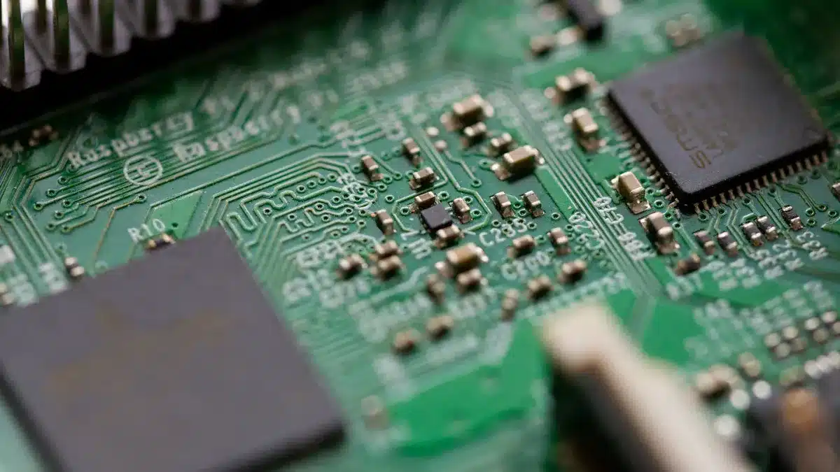
Multilayer PCBA has three or more copper layers. Insulating layers go between each copper layer. This lets you fit many circuits in a small space. You see multilayer PCBA in advanced devices like smartphones and wearables. It supports fast data and complex features.
Here is a table that lists the good and hard parts of multilayer PCBA:
Aspect | Benefits | Challenges |
|---|---|---|
Reliability | Strong bonding, resists heat, vibration, and moisture | Needs precise manufacturing and advanced equipment |
Design Flexibility | Supports complex layouts and last-minute changes | Skilled designers needed to manage connections and signal issues |
Form Factor | Smaller size, integrates many functions | |
Electrical & Thermal Performance | Improved signal quality, noise isolation, and heat dissipation | Harder to repair due to hidden layers |
Cost | Reduces material and labor costs for complex devices | Higher initial manufacturing cost |
Manufacturing Evolution | Advanced tech improves quality and yield | Limited manufacturer availability |
Multilayer PCBA lets you pack more parts in less space.
Devices get smaller and lighter with more features.
Making these boards takes longer and needs skilled workers.
Fixing multilayer PCBA is hard because layers are hidden.
Flexible PCBA
Flexible PCBA uses bendy materials like polyamide. You can twist or fold these boards. They do not break easily. Flexible PCBA is important for foldable phones and smartwatches. Medical devices use it too. The design fits in tight or curved places.
Flexible PCBA is light, stretchable, and safe for the body.
You see it in wearable sensors and health patches.
Special metal shapes help it work better and bend more.
Flexible PCBA lets you make devices that fit the body or wrap around things.
Tip: Flexible PCBA is growing fast. More mobile devices will use it for new shapes and features.
Rigid PCBA
Rigid PCBA uses hard materials like fiberglass. The board stays flat and does not bend. Most phones, laptops, and machines use rigid PCBA. It gives strong support for heavy parts.
Metric | Value |
|---|---|
2.1% | |
Post-implementation field failure rate | 0.3% |
Average cost per field failure | $4,200 |
Annual production | 50,000 units |
Initial investment in testing | $175,000 |
Annual operating cost | $120,000 |
Annual savings from reduced failures | $378,000 |
First-year ROI | 47% |
Rigid PCBA meets high standards for safety and quality.
Testing lowers the chance of failure and saves money.
Use rigid PCBA when you need strong and steady boards.
Rigid-Flex PCBA
Rigid-Flex PCBA mixes hard and bendy parts in one board. You get the strength of rigid and the bend of flexible PCBA. This is great for foldable phones and cameras. Medical devices use it too.
Rigid-Flex PCBA bends and folds better than just rigid boards.
It helps with heat and lowers stress on parts.
You can use it in small spaces where other boards do not fit.
Studies show rigid-flex PCBA works well even when bent many times.
Note: Rigid-Flex PCBA gives you strong, small, and reliable devices for modern needs.
HDI and Advanced PCBA
HDI PCBA
You can find HDI in many new devices. HDI stands for High-Density Interconnect. It uses new technology to fit more parts on a printed circuit board. This helps make your device smaller and lighter. It also makes it work faster. HDI PCBA is special because it has thinner lines and smaller holes. It also uses special ways to connect parts. You can put more circuit tracks and parts in a tiny space. This is a big reason why people like hdi pcbs. The hdi pcb manufacturing process uses microvias, blind vias, and buried vias. These things help you add more parts and get better electrical performance.
HDI pcb design can use line widths as small as 2/2 mil.
You can make boards with up to 10 layers and keep them thin, under 0.8mm.
The hdi pcb manufacturing process makes the board lighter and smaller.
Note: HDI PCBA gives you better signal quality. It also works well with fast connections like 5G.
HDI PCB Design
When you use hdi pcb design, you need to follow special rules. The stackup, or how the layers are set up, can change for each project. You can pick from different stackup types:
1+N+1: Two hdi layers are on the outside of N normal layers. This gives a good mix of cost and performance.
2+N+2: Two hdi layers are on each side of N normal layers. This lets you make more complex circuits.
ELIC: Every Layer Interconnection. This gives you the most options and is used in aerospace.
You need to think about the space between layers and the materials you use. These choices help stop signal loss and make the board work better. Changing copper thickness in power and ground layers helps power flow better. Good hdi pcb design makes signals stronger, gives better power, and helps control heat.
Applications of HDI PCBs
You can find applications of hdi pcbs in many areas. HDI boards are used in smartphones, medical devices, and car electronics. These things need to work well and use new technology. HDI pcb design lets you add more features in a small space. You also get better reliability and longer-lasting boards, which are important benefits of hdi pcbs.
HDI PCBs can handle fast data and hard tasks.
You see them in devices that need to be strong.
HDI PCBs help save space and make things work better.
Tip: HDI PCBA is the best choice for small, high-performance devices.
PCBA Comparison
Key Differences
There are big differences between a pcb and a pcba. A pcb is just a board with copper lines. It cannot work by itself. A pcba has all the parts added, so it works in your device. The table below shows how they are not the same:
Aspect | PCB (Bare Board) | PCBA (Assembled Board) |
|---|---|---|
Definition | Non-functional board with copper traces only | Functional board with electronic components mounted |
Functionality | Passive support and routing | Active assembly performing electronic tasks |
Complexity | Simple design with layers and copper pathways | Complex due to component mounting and soldering |
Manufacturing | Fabrication of board only | Assembly including SMT or Thru-Hole component placement, soldering, inspection, and testing |
Applications | Base for circuit assembly | Used in fully functional devices like smartphones, medical equipment, automotive systems |
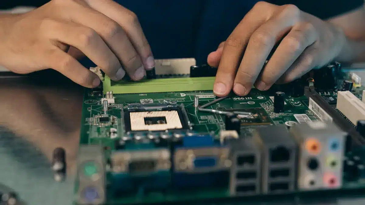
You will also notice differences with surface-mount technology and thru-hole technology. SMT puts parts on top of the board. This makes the board smaller and lighter. Thru-hole puts parts through holes in the board. This makes strong connections for heavy-duty uses.
Pros and Cons
Each pcba type has good and bad points. Here are some important things to know:
Single-layer pcb: Easy to make and cheap. Not good for complex hdi or fast work.
Double-sided pcb: More connections and better than single-layer. Still not enough for very advanced uses.
Multilayer pcb: Good for high-density hdi and small design. Great for phones and wearables. Harder to fix and costs more.
Flexible pcb: Bends and fits in tight spaces. Great for foldable phones and wearables. Needs special materials and careful planning.
Rigid-flex pcb: Mixes strong support with bending. Works well in tough places. Harder to make.
Tip: Always pick the pcba type that matches your device’s needs. This gives you the best performance and reliability.
Application Suitability
You need to choose the right pcba for your device. Multilayer pcb and hdi are best for phones and advanced electronics. Flexible pcb is good for foldable phones and wearables. Rigid-flex pcb gives both strength and bending for medical and mobile uses.
You can trust these boards because they pass many tests. Engineers use heat, humidity, and shaking tests to check if they last. They also use burn-in and high-heat tests to make sure the pcba will work for a long time. Automated checks and x-ray tests help find problems in the design or build.
Each pcba type fits certain uses. Single-layer and double-sided pcb are for simple electronics. Multilayer, flexible, and rigid-flex pcb are for high-density hdi and advanced mobile devices.
Choosing Mobile PCBA
Selection Criteria
When you pick a mobile pcba, you must think about many things. Every device is different and needs special care. You want your device to work its best. First, look at what parts your device uses. Microprocessors, capacitors, and resistors must be put in the right spots. This helps signals stay strong and keeps the board cool.
You also need to keep signals clear. Good grounding and shielding help your data move fast and safe. Matching impedance and using differential signals can lower noise. The board material matters a lot too. FR4 is good for most boards. Polyimide is better if you need a flexible board. PTFE or ceramic help with high heat or fast signals.
How you make the board is important. HDI and microvia tech let you fit more parts in a small space. This is needed for new phones and wearables. Pick the pcba type—flexible, rigid-flex, or multilayer—that fits your device’s shape. Good assembly, like careful SMT and reflow soldering, helps your board work well.
Here is a table that lists the main things to check:
Criteria Category | Key Considerations | Impact on PCBA Selection and Device Performance |
|---|---|---|
Component Types | Placement and routing | Signal integrity, heat, power |
Signal Integrity Management | Grounding, shielding, impedance, differential lines | Reliable high-speed data, less noise |
Materials | FR4, polyimide, PTFE, ceramic | Durability, flexibility, thermal stability |
Manufacturing Techniques | HDI, microvia | Miniaturization, signal integrity |
PCB Types | Flexible, rigid-flex, multilayer | Adaptability, weight, integration |
Assembly Best Practices | SMT, reflow, automation | Reliable connections, fewer defects |
Power Management | Voltage regulators, capacitors, PMICs | Power efficiency, heat, device life |
Tip: Big companies like Apple and Samsung use these steps to get the best hdi pcba for their devices.
Practical Tips
You can make smart choices for your device by following these tips:
Know Your Device Needs
Write down what your device must do. Think about size, speed, and battery life. This helps you pick the right pcba and hdi features.Work With Experts
Talk to engineers who know about hdi and advanced pcba. They can help you avoid mistakes and improve performance.Test Early and Often
Use tests for heat, vibration, and signal quality. Early testing finds problems before they become big issues in your applications.Choose the Right Manufacturer
Pick a company with experience in hdi and mobile pcba. Look for good reviews and strong quality checks.Plan for the Future
Think about new hdi technology and how it can help your next device. Stay updated on trends in mobile applications.
Remember: The right pcba and hdi design can make your device work better and last longer. Always match your board to what your device really needs.
PCBA Summary Table
You have learned about different mobile PCBA types. This summary table lets you compare them fast. It shows the main features, good points, and best uses for each type. You can check this table when picking a PCBA for your device.
PCBA Type | Structure | Key Features | Typical Applications | Pros | Cons |
|---|---|---|---|---|---|
Single-Layer | 1 copper layer | Simple, low cost | Remote controls, LED lights | Easy to make, cheap | Limited functions |
Double-Sided | 2 copper layers | More connections | Tablets, audio devices | Better performance | Harder to repair |
Multilayer | 3+ copper layers | Compact, high density | Smartphones, wearables | Saves space, fast signals | Expensive, complex |
Flexible | Bendable materials | Can twist and fold | Foldable phones, sensors | Fits tight spaces | Needs special materials |
Rigid | Hard, flat materials | Strong, stable | Laptops, mainboards | Durable, reliable | Cannot bend |
Rigid-Flex | Mix of rigid and flexible | Bends and supports | Cameras, medical devices | Small, strong, flexible | Costly, complex to make |
HDI | High-density layers | Tiny lines, microvias | 5G phones, advanced devices | High speed, miniaturized | Needs advanced tools |
Tip: Check this table to match your device with the right PCBA. HDI boards are best for small and fast devices.
If you want a thin and strong device, look at hdi PCBA. For easy gadgets, single-layer or double-sided boards are good. Flexible and rigid-flex boards help you make new shapes and wearables.
You can use this summary as a checklist. It helps you pick the best PCBA for your next project.
You can pick from many PCBA types, like single-layer, flexible, and hdi. Each type is good for different devices. Flexible and hdi boards are best for small, fast gadgets. Rigid-flex gives both strength and bending. Always choose a PCBA that fits your device’s needs. Use this checklist when picking a PCBA:
Choose advanced types like flexible, multilayer, or hdi for small, strong devices.
Think about adding AI and IoT features.
Pick materials that are better for the environment.
Look at what local factories do best.
The PCBA market is getting bigger. New hdi designs, smart features, and green materials will change mobile devices in the future.
FAQ
What is the main difference between a PCB and a PCBA?
A PCB is just the board with copper lines. A PCBA has all the electronic parts attached. You need a PCBA to make your device work.
Why should you choose HDI PCBA for mobile devices?
HDI PCBA lets you fit more parts in a small space. You get faster speed and better performance. Your phone or wearable can be thinner and lighter.
Can flexible PCBA break easily?
Flexible PCBA uses strong, bendy materials. You can twist or fold it many times. It does not break easily if you use it the right way.
How do you pick the right PCBA type for your device?
Make a list of what your device needs. Think about size, speed, and shape. Choose a PCBA that matches these needs. Ask experts if you feel unsure.
What tests help make sure your PCBA works well?
Heat tests
Vibration tests
X-ray checks
These tests help you find weak spots. You can fix problems before your device goes to market.
See Also
Benefits And Obstacles Of Flex PCBA In Electronics
A Comprehensive Look At Android PCBA In Technology
How PCBA Enhances Modern Electronics Through Various Uses
Creating Tailored Android PCBAs To Meet Device Demands
Investigating Testing Methods For PCBA In Electronics Production