Optimizing your circuit board layout greatly affects how well your device works. Placing components correctly can lower interference and improve functionality. Good routing makes sure electrical connections are reliable. Also, paying attention to thermal management stops overheating. Each of these parts is very important for your design’s overall efficiency.
Here’s a quick look at how these main parts affect device performance:
Impact on Device Performance | |
|---|---|
Component Placement | Improves performance and reduces interference. |
Routing | Makes sure electrical signals have efficient connections. |
Thermal Management | Stops overheating and helps the device last longer. |
By focusing on these things, you can make a better and more reliable circuit board layout.
Key Takeaways
Placing components correctly helps reduce interference. It also improves signal quality. Keep related components close to make connections easier.
Keep trace lengths short to improve signal quality. Short traces lower resistance and reduce electromagnetic interference. This helps overall performance.
Good routing is important for strong signals. Use equal trace lengths and avoid sharp turns. This keeps the signal clear.
Use ground planes to reduce noise and improve power delivery. They give stable reference points for signals. This makes them more reliable.
Regularly testing and prototyping helps find design problems early. Follow a clear testing process. This ensures your circuit board works well.
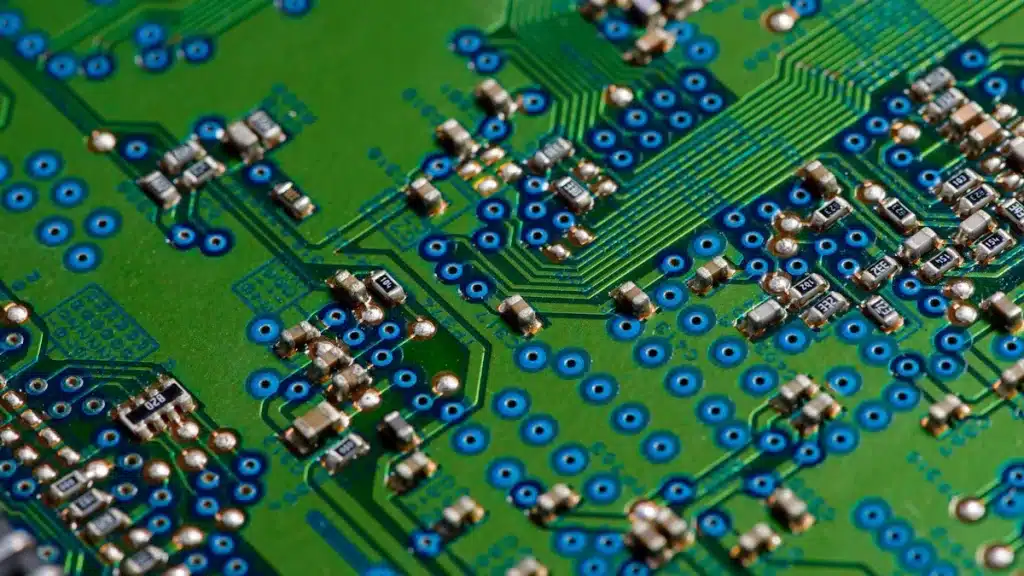
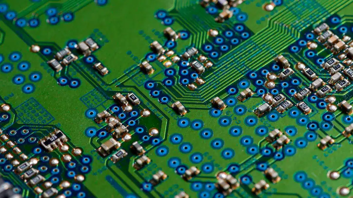
Component Placement in PCB Design
Placing components correctly is very important in PCB design. It affects how well your circuit board works and how reliable it is. When you put components in the right spots, you can reduce interference and improve signal quality.
Grouping Related Components
Putting related components together makes your design easier and better. When you keep parts that work together close, you need shorter traces to connect them. This saves space and cuts down on signal loss.
First, find components that often interact.
Place connectors, switches, and other fixed parts first. These need specific spots and help shape the layout.
After placing fixed parts, put related components nearby. This makes routing and power distribution easier.
By improving your component placement, you can lower manufacturing costs and make PCB design simpler. A neat layout reduces routing problems and board size, leading to a better circuit board design.
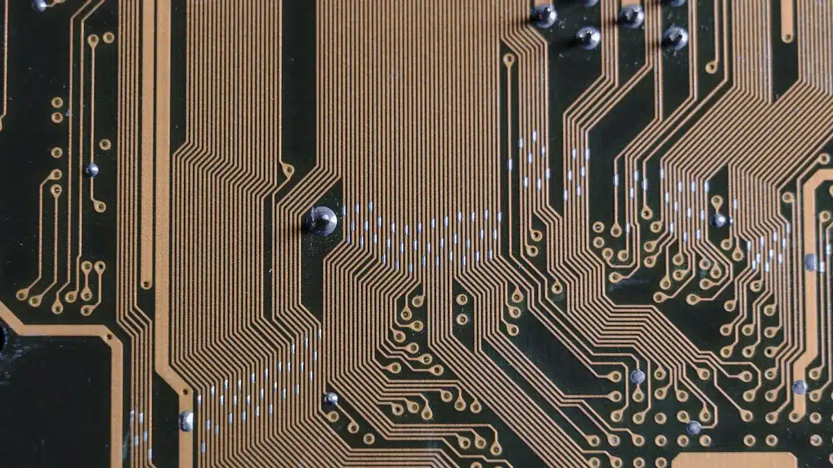
Minimizing Trace Length
Keeping trace length short is key for good signal quality. Long traces can add unwanted resistance and inductance. This can cause voltage drops and electromagnetic interference (EMI).
In fast designs, even a small stub (0.5 mm) can cause big problems, like signal delay or impedance mismatch. This messes up the 50-ohm impedance in high-frequency circuits.
Shortening power traces lowers inductance, which helps keep voltage levels steady and reduces EMI.
To keep trace length optimal, follow these tips:
Align the lengths of multiple traces that run parallel. This is called PCB trace length matching.
For digital signals, figure out critical lengths based on rise time and signal speed. For example, if the signal rise time is 1 ns and the signal speed is 6 inches/ns, the critical length is 3 inches. Traces shorter than 2 inches help reduce signal delay and impedance mismatch.
By focusing on trace length, you boost the overall performance of your circuit board layout.
Effective Routing for Circuit Board Layout
Routing traces on your circuit board is very important. It helps keep signals clear and strong. Good routing makes sure electrical signals move well and without problems. When you design your PCB layout, think about these key points to make it better.
Signal Integrity Considerations
To keep signals strong, follow these tips when routing PCB traces:
Equal Trace Lengths: Make clock signals the same length. This helps data travel together.
Avoid Branches: Don’t use branches in your traces. This helps stop reflections. Use a clock driver to send the signal out.
Impedance Matching: Add impedance-matching resistors to clock signals. This helps match the output with the trace.
Signal Layers: Put signal layers between ground planes. This gives a low-resistance path, which is important for fast signals.
Material Selection: Pick materials with low dielectric constants. Use controlled impedance routing to improve signal quality.
Microvias Placement: Place microvias close to signal pads. This helps reduce reflections and keeps signals strong.
Decoupling Capacitors: Put decoupling capacitors near power pins. This helps keep power steady and cuts down noise.
Guard Traces: Use guard traces to lessen crosstalk between nearby signals.
Shielding Techniques: Use shielding methods and a solid ground plane to reduce electromagnetic interference (EMI) and compatibility issues.
Bad routing can cause big problems for signals, especially in fast circuit boards. Sharp turns or too much twisting in traces can hurt signal quality. To keep signals clear, design traces to turn smoothly. This is very important for fast signals, which can act like antennas if not handled well.
Using Ground Planes
Ground planes are very important for making your circuit board work better. They give low-resistance paths for return currents. This helps cut down noise and keep signals clear. Here are some benefits of using ground planes:
Noise Reduction: Ground planes help lower noise, which is important for good designs.
Signal Integrity: They keep signals strong by giving a stable reference point.
Power Delivery: Ground planes help with power delivery and heat management, stopping problems like brown-outs.
When you design your PCB layout, make sure to use ground planes well. This will not only make your circuit board better but also make your device more reliable.
By focusing on good routing and using ground planes, you can greatly improve your circuit board layout. These tips will help you create a more reliable and efficient PCB design.
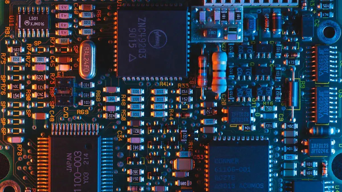
Printed Circuit Board Design Dimensions
Setting the size of your printed circuit board design is very important. The shape and size of your PCB can greatly affect how well it works and how easy it is to make. You need to think about how the size impacts the layout and design of your circuit board.
Layer Configuration
Layer configuration is key in fast digital applications. A smart setup of layers helps signals travel without problems. Here’s a good layer setup for multilayer PCBs:
Layer | Purpose | Material |
|---|---|---|
Top Layer | Signal layer | Copper/FR4 |
Ground Plane | Noise reduction | Copper |
Power Plane | Power distribution | Copper |
Signal Layer | Routing data signals | Copper/FR4 |
Bottom Layer | Signal layer | Copper/FR4 |
In fast applications, placing ground and power planes correctly creates a stable area. This reduces noise and improves performance. You should try to balance the number of layers with the need for strong signals. More layers can help performance but also raise manufacturing costs. For example, changing from a 2-layer to a 4-layer PCB can increase costs by 30-40%.
Thermal Management
Good thermal management is key to stopping overheating in crowded circuit boards. You can use several methods to control heat well:
Do early thermal checks to find overheating risks.
Use heat sinks, thermal vias, and forced air cooling together.
Place components wisely to avoid hot spots and spread heat evenly.
By keeping high-power parts away from heat-sensitive ones, you can lower the risk of thermal coupling. This helps heat move away better and makes your PCB design more reliable. Remember, 18% of PCB prototype failures come from ignoring thermal design. So, focusing on thermal management can greatly boost your circuit board’s performance and lifespan.
By paying attention to layer configuration and thermal management, you can improve your PCB layout for better performance and reliability.
Verifying Your Circuit Board Design
Checking your circuit board design is very important. It helps make sure your board works well and is safe. You must follow certain design rules. This will help you avoid problems that could make your board hard to build or unsafe. Using best practices helps you meet industry standards. This is key for making your board safely.
Prototyping and Testing
Making a prototype and testing your circuit board design helps you find and fix mistakes early. Here are the main steps in this process:
Define test objectives: Say what you want to learn from testing.
Identify test cases: Look at performance factors like voltage tests and I/O checks.
Specify the testing environment and tools: List the conditions and tools needed for testing.
Define the pass/fail criteria: Set clear rules for what is acceptable.
Document the steps: Write down the order of tests.
Execute unit-level and integration tests: Test single parts and how they work together.
Generate a test report: Summarize results, failures, and if they meet standards.
Refine the prototype: Change the design based on test results.
Execute final functional testing: Check the whole board in real-world situations.
Perform EMC and safety tests: Make sure it meets industry rules.
By doing these steps, you can lower the chance of problems in your PCB layout.
Analyzing Performance Metrics
After testing, you should look at different performance metrics. This helps you check the quality of your circuit board design. Here are some important metrics to think about:
First Pass Yield (FPY): Shows the percentage of products that pass all quality checks during the first assembly.
Defect Rate: Tells you the percentage of bad units made, showing where to improve.
Cycle Time: Total time to put a product together; shorter times mean better efficiency.
Throughput: Number of units made in a certain time; this is key for keeping quality.
Overall Equipment Efficiency (OEE): Looks at how well the equipment works during assembly.
By checking these metrics, you can make sure your circuit board design meets the needed standards for performance and reliability. Remember, finding design problems early can stop expensive redesigns and delays.
Making your circuit board layout better is very important for good performance and reliability. You might have problems like more complex PCBs and making sure manufacturers understand your design. To fix these issues, pay attention to these main strategies:
Mechanical Layout: Make sure bends in flexible PCBs are smooth. This helps them last longer.
Stack-Up Optimization: Align copper layers correctly to reduce stress.
Utilize Advanced Tools: Use automation and real-time checks to cut down on mistakes and design time.
By using these ideas, you can create designs that work well and meet industry standards. A well-made PCB not only works better but also lowers production costs and time. 🌟
FAQ
What is a PCB layout?
A PCB layout is how you arrange electronic parts and their connections on a printed circuit board. You create it to make sure everything works well, signals are clear, and heat is managed.
Why is component placement important?
Component placement is key for your PCB layout’s efficiency. Placing parts correctly cuts down on interference and keeps trace lengths short. This leads to better signal quality and overall performance.
How can I improve signal integrity?
To boost signal integrity, match trace lengths, avoid sharp turns, and use ground planes. These steps help keep signals strong and reduce noise in your PCB layout.
What role does thermal management play?
Thermal management stops overheating in your PCB layout. You can do this by using heat sinks, thermal vias, and placing components wisely to spread heat evenly.
How often should I prototype my design?
You should prototype your design at different stages. Early prototyping helps find problems quickly, letting you improve your PCB layout before final production.
See Also
Essential Strategies to Enhance PCB Assembly Productivity
Best Practices for Achieving Quality and Efficiency in PCBA
Ways to Optimize Workflow Efficiency in PCBA Production
Ten Professional Suggestions for Cost-Effective PCBA Assembly