
A printed circuit board, commonly known as a PCB, is essential in modern electronics. The pcb definition refers to a board that serves as the main support for devices like smartphones, tablets, and smartwatches. You rely on PCBs to connect various electronic components, ensuring your devices function properly. Nearly all contemporary electronic devices use PCBs for these connections. Over the past decade, advancements in PCB technology have made devices smaller, more reliable, and enhanced their portability and performance.
Key Takeaways
PCBs are the main part that holds and connects electronic pieces. They help devices work well and reliably.
Different materials like FR-4, polyimide, and Teflon change how PCBs manage heat, flexibility, and electrical signals.
PCBs have many layers. These include copper paths and protective coatings. They help signals move easily and protect the board.
There are different types of PCBs. Single-sided ones are for simple devices. Multi-layer ones are for advanced electronics like smartphones.
Good PCB design and proper placement of parts make devices work better. They also make them last longer and allow for smaller, more powerful gadgets.
PCB DEFINITION
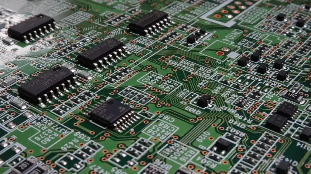
A printed circuit board (PCB) is very important in electronics. It acts as a base for putting together electronic parts and their connections into one circuit. Usually, a PCB has a nonconductive base that can be stiff or bendable. It also has conductive paths that link different parts. This design helps signals and power move easily in electronic devices.
The materials used in PCBs are very important for how they work. Often, makers use materials like FR-4, which is made of woven fiberglass and epoxy resin. This material has great mechanical and electrical features, making it perfect for most consumer electronics. Other materials, like polyimide laminates, are flexible and can handle high heat, which is good for things that need to bend or fold.
Here’s a quick overview of some commonly used materials in PCB construction:
Material | Description | Key Properties | Suitability |
|---|---|---|---|
FR-4 | Composite of woven fiberglass cloth and flame-resistant epoxy resin | Excellent mechanical, electrical, thermal properties; good strength-to-weight ratio | Ideal for lightweight, rigid PCBs used in most consumer electronics |
Polyimide laminates | Flexible laminate used in rigid-flex PCBs | High thermal stability, dimensional stability during thermal cycling, flexibility | Suitable for harsh, high-temperature environments and multi-layer flexible PCBs |
Teflon (PTFE) | Material with excellent dielectric properties | Low dielectric constant, minimal resistance, lightweight, flexible | Preferred for high-speed, high-frequency circuits despite higher cost |
The design of a PCB is very important for how it works. A typical PCB has a flat insulating base with copper foil on it. Makers use chemical etching to create conductive lines, called traces, pads, and vias, which connect parts and layers. These traces work like fixed wires, separated by the base. Protective coatings, like solder masks, stop corrosion and short circuits.
PCBs come in different types, like single-sided, double-sided, and multilayer designs. Single-sided PCBs have one conductive layer and are often used in simple, low-cost electronics. Double-sided PCBs can have more complex circuits because they have copper traces on both sides. Multilayer PCBs have three or more layers, allowing for high-performance uses in small spaces.
The importance of PCBs in electronic devices is huge. They give a strong base for holding and connecting parts, allowing for compact and efficient designs. PCBs support complex functions, help with mass production accurately, and improve durability and performance. In consumer electronics like smartphones, tablets, and computers, PCBs make sure everything works smoothly and connects well.
COMPOSITION OF PRINTED CIRCUIT BOARDS
MATERIALS USED
Printed circuit boards (PCBs) use different materials to work well and last long. The most common non-conductive materials are:
FR-4: This is a fiberglass and epoxy mix. It resists fire and provides good electrical insulation. It can handle high heat and is affordable.
Polyimide: This material can tolerate high temperatures, up to 400°C. It has great mechanical and electrical features, making it perfect for flexible PCBs.
Teflon (PTFE): This non-conductive material gives excellent thermal and electrical insulation. Its low dielectric constant makes it good for high-frequency uses.
Ceramic materials: These include alumina and aluminum nitride. They have high thermal conductivity and low thermal expansion. They are often used in high-power devices.
These materials are very important for how PCBs perform in heat and strength. For example, FR-4 has a thermal expansion rate of about 11 ppm/°C. In contrast, aluminum nitride ceramics have lower rates, which helps keep their shape when temperatures change.
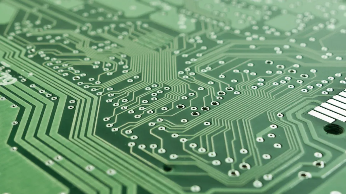
LAYERS OF A PCB
A PCB has many layers, and each one has a special job. A typical PCB layout includes:
Copper Layers: These layers create the paths that connect different PCB parts. The thickness of the copper affects how well signals travel and how strong the device is. Thicker copper lowers resistance and boosts current flow, while thinner copper helps with matching impedance at high frequencies.
Insulating Layers: These layers are usually made from prepreg and laminate materials. They provide electrical insulation and keep the structure strong. They connect the copper layers and core materials, affecting signal loss and weakening. Choosing the right insulating materials is key for keeping high-speed signals clear.
Solder Mask: This layer protects the copper traces from rust and damage. It also helps prevent short circuits during soldering.
Multilayer PCBs, often found in smartphones and laptops, usually have between 4 and 12 layers. This layered design allows for complex circuits in small spaces, improving device performance and reliability.
FUNCTIONS OF PCBS
ELECTRICAL CONNECTIONS
Printed circuit boards (PCBs) are very important for making electrical connections between different electronic parts. They act like a base where integrated circuits (ICs) and passive parts, like resistors and capacitors, connect easily. You can think of the PCB as a road for electrical signals. It helps them move quickly from one part to another.
Here are some key features of PCBs that help with these electrical connections:
Conductive Traces: These copper paths connect ICs and passive parts. They work like wires, making sure signals flow correctly in the circuit. For example, copper traces link the pins of an IC to resistors and capacitors, helping the circuit work as it should.
Connectors: These parts let your PCB connect physically and electrically with other devices. Common types include USB ports, HDMI connectors, and pin headers. They make sure your PCB can talk to outside devices well.
IC Sockets: These sockets let you easily put in and take out ICs without soldering. This is very helpful for testing and fixing, allowing you to change parts when needed.
Component Placement: How components are arranged on the PCB is very important. A good layout makes sure signals flow well and keeps everything stable. You want to place ICs close to their related passive parts to reduce signal loss.
Package Types: Different package types change how parts connect to the PCB. Through-hole technology (THT) is good for easy testing, while surface-mount technology (SMT) allows for more compact assembly.
The design of the PCB layout affects how well the circuit works. For example, bad placement can cause signal problems or higher resistance, which can hurt how your electronic device functions.
MECHANICAL SUPPORT
PCBs also give important mechanical support for electronic parts. They keep parts in place, making sure they stay secure while working. This support is crucial for keeping the circuit safe, especially in devices that face physical pressure.
There are two main ways to mount parts on PCBs:
Through-Hole Technology (THT): This method drills holes in the PCB where component leads go in and are soldered on the other side. This makes a strong bond, making THT great for uses in cars and planes where parts face a lot of stress.
Surface-Mount Technology (SMT): SMT places parts directly onto PCB pads with solder. While this method allows for smaller parts and more density, it usually gives less mechanical strength than THT. However, SMT is popular in consumer electronics because it is efficient for assembly.
Many modern PCBs use a mix of both THT and SMT. This method improves mechanical support while keeping things compact. For example, you might use THT for bigger parts that need strong support and SMT for smaller, tightly packed parts.
TYPES OF PCBS AND APPLICATIONS
SINGLE-SIDED PCBS
Single-sided PCBs are the easiest type of printed circuit board. They have copper traces on just one side of the board. This makes them simple to design and make. Here are some key features of single-sided PCBs:
Description | |
|---|---|
Conductive Layer | Copper traces are only on one side, making layout and manufacturing easier. |
Component Placement | Components can go on both sides, but only one side has traces. |
Interconnects | Uses plated through holes for connections; no internal layers. |
Interconnect Density | Limited because of one conductive layer, which restricts complex routing. |
Performance | Lower limits for high frequency, fast logic, and impedance control than multilayer PCBs. |
You can find single-sided PCBs in many low-cost products. Common uses include toys, basic appliances, and lighting fixtures. They are also used in power and analog circuits, like isolated converters and simple radio frequency applications. Their low costs make them great for quick prototypes and hobby projects.
MULTI-LAYER PCBS
Multi-layer PCBs have several layers of copper separated by insulating material. This design allows for more circuits and better performance in advanced electronics. Here are some important features of multi-layer PCBs:
They allow compact designs, fitting more parts into smaller spaces.
The layered structure cuts down on electromagnetic interference, improving signal quality.
Multi-layer PCBs support high-density assemblies, which are important for devices like smartphones and laptops.
You will see multi-layer PCBs in many applications, especially in telecommunications and computing equipment. They are used in motherboards, graphics cards, and servers, where high performance and space-saving features are very important. In telecommunications, multi-layer PCBs are crucial for devices like routers, satellites, and mobile phones, providing strength and functionality.
The growth of multi-layer PCB technology has greatly affected modern electronics. As devices get smaller and more complex, the need for multi-layer PCBs keeps increasing, making them a key part of today’s electronic world.
In conclusion, printed circuit boards (PCBs) are very important in today’s electronics. They give a strong base for connecting and holding electronic parts. Here are some main points to remember:
PCBs make things simpler and save space compared to manual wiring.
They have many layers, like a base, copper paths, and protective coatings.
Different kinds of PCBs, like single-sided and multilayer boards, fit different uses.
Design choices, like where to place parts and how to route traces, are key for good performance and reliability.
In general, PCBs improve how devices work, help make them smaller, and ensure they are reliable in many fields, from consumer electronics to aerospace.
FAQ
What is the main purpose of a PCB?
A PCB connects electronic parts and helps them work together. It gives a strong base for parts, making sure they work well in devices like smartphones and computers.
How are PCBs manufactured?
Manufacturers make PCBs by stacking materials, adding copper, and carving designs. They then put on protective coatings and solder pads to make them last longer and work better.
What are the advantages of multi-layer PCBs?
Multi-layer PCBs save space and cut down on interference. They allow for complex circuits in small designs, making them perfect for advanced electronics like laptops and smartphones.
Can I design my own PCB?
Yes, you can design your own PCB using software tools. Many programs have easy-to-use interfaces, letting you create layouts and test circuits before making them.
What is the difference between THT and SMT?
Through-Hole Technology (THT) means putting leads through holes in the PCB, making strong connections. Surface-Mount Technology (SMT) places parts directly on the board, allowing for smaller designs and more parts.
See Also
Exploring What PCBA Means And Its Importance In Electronics
A Clear Guide To PCBA Definition And Its Uses In Electronics
Defining PCBA And Explaining Its Function Within Electronics