
The fast growth of technology makes PCBA design for manufacturability very important. Keeping up with 2025 trends is now a must to stay competitive. Industries like electronics, cars, and telecom are asking for better PCBs. Companies such as Dixon Technologies have seen big success, with a 117% revenue jump. This shows the rising need for powerful designs. Flexible and rigid-flex PCBs are becoming popular. They save space and work well for wearables and car tech.
As new ideas change PCBA design for manufacturability, AI and better materials help makers meet the need for faster and smarter devices.
Key Takeaways
Use smaller parts and dense connections in PCB designs to stay ahead. These help make tiny, smart devices for today’s tech needs.
Try flexible and rigid-flex PCBs to make devices more useful. These are important for industries like electronics and healthcare, creating cool products like foldable phones and wearables.
Use AI tools to make PCB production faster and better. AI finds problems early, makes work easier, and improves product quality.
Go green with eco-friendly manufacturing to attract caring customers. Using safe materials and recycling helps the planet and your brand.
Use 3D printing to quickly test ideas and make tricky designs. This saves money and speeds up making products, so they sell faster.
Key Trends in PCBA Design for Manufacturability
Miniaturization and High-Density Interconnects
Smaller and smarter devices are in high demand today. This has led to making PCBs smaller and packing more parts into them. High-density interconnect (HDI) PCBs are now very important. They let makers fit more parts into tiny spaces. This helps create small designs that still work well. Industries like electronics and IoT use HDI PCBs for gadgets like smartwatches and home systems.
New tech in HDI PCBs is helping the market grow. For example:
Efficient routing keeps signals clear and reduces problems.
Ground and power planes make signals stronger and more stable.
Thermal management stops parts from overheating, making them last longer.
The rise of IoT and 5G has made miniaturization even more important. IoT gadgets need small designs to fit sensors and wireless parts. 5G needs fast PCBs to handle lots of data. So, makers are working hard to improve HDI PCB designs to meet these needs.
Flexible and Rigid-Flex PCBs for Modern Applications
Flexible and rigid-flex PCBs are changing how devices are made. They are light, strong, and save space. These PCBs are very useful in industries like electronics, cars, and healthcare.
In electronics, flexible PCBs allow cool designs like foldable phones and curved screens. For example, one company used flexible PCBs to make a foldable phone with two screens. Wearables like fitness trackers also use flexible PCBs for better comfort and function.
Cars use rigid-flex PCBs for important systems like airbags and navigation. These PCBs handle bumps and shocks, working well in tough conditions. In healthcare, flexible PCBs are used in devices like pacemakers and monitors. They are adaptable and reliable for patient care.
More companies are using flexible and rigid-flex PCBs. They help make devices smaller, stronger, and more versatile. These PCBs are shaping the future of technology.
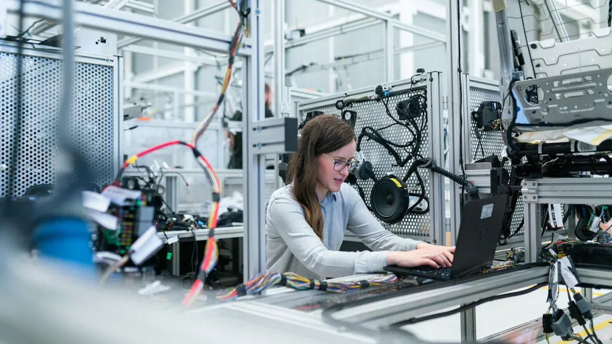
AI-Driven Design and Automation in PCBA
Artificial intelligence (AI) is changing how PCBs are designed and made. AI tools make the process faster and more accurate. For example, machine learning can find signal problems and suggest fixes. This helps create better PCBs.
Big companies like Siemens and Flex are using AI in their work. Siemens Valor AI finds defects during assembly, cutting waste and saving time. Flex uses AI to improve production lines, saving money and boosting efficiency.
AI also helps with maintenance and smart factories. Jabil, a global company, uses AI to check machines and avoid breakdowns. This improves how factories run.
By automating boring tasks, AI lets designers focus on new ideas. Adding AI to PCB design speeds up work and ensures high-quality PCBs are made.
Sustainable Manufacturing Practices in PCBA
Sustainability is now a key part of PCB design. Companies use eco-friendly methods to protect the environment and stay efficient. This change matches global moves toward green tech and strict rules.
One way is using lead-free solder and halogen-free laminates. These materials lower toxic waste and follow rules like RoHS. Makers also try water-based cleaners instead of chemical ones to cut harmful emissions.
Recycling is very important in sustainable PCBA work. Many companies recycle scraps like copper and laminate pieces to reduce trash. Some even reuse water and chemicals with closed-loop systems during production.
Saving energy is another big focus. Energy-efficient machines and better production setups help lower carbon footprints. Smart factories with IoT sensors track energy use and make changes to save resources.
Tip: Green practices help the planet and improve brand image. They also attract customers who care about the environment.
Advanced Materials for High-Speed Applications
Fast data needs have pushed PCB designs to improve. Old materials like FR4 don’t work well for high-frequency uses. New materials now offer better performance and reliability.
Polyimide and low-loss substrates are vital for fast PCBs. They keep signals clear and reduce distortion. These materials also handle heat well, making them great for telecom and data centers.
Designers add embedded capacitors and power planes to PCBs. This lowers noise and improves power flow, which is key for fast circuits. These features help devices work better without getting bigger.
The market for high-speed boards is growing fast. Reports show more companies use advanced materials for faster, reliable devices. This proves how important new materials are for PCB progress.
Note: Using advanced materials costs more at first. But the better performance and reliability make it worth the price later.
The Role of 3D Printing in PCB Assembly
Speeding Up Prototyping with 3D Printing
3D printing has changed how PCBs are made for testing. Old methods take time because they need special tools and setups. With 3D printing, designers can quickly make PCBs for specific needs. This helps companies test and improve designs faster before making many copies.
Quick design changes help companies stay ahead in technology. For example, wearable tech makers use 3D printing to create small PCBs for smartwatches. By making prototypes faster, businesses can release products sooner and compete better.
Tip: Using 3D printing for prototyping saves time and avoids mistakes. It also reduces waste and costs.
Making Complex PCB Designs Possible
Modern devices need very detailed PCBs for advanced features. 3D printing allows creating tricky shapes that old methods can’t do. Designers can add layers, special parts, and unique shapes without losing quality.
This is helpful for industries like space and healthcare. Space engineers use 3D printing for light PCBs in satellites. Medical device makers use it for tiny PCBs in implants.
3D printing also allows custom designs for special needs. Designers can try new layouts and materials, leading to better PCBs.
Callout: 3D printing helps make smarter devices with advanced designs for today’s needs.
Saving Money and Time in PCB Making
3D printing makes PCB production cheaper and faster. It removes the need for costly tools and reduces wasted materials. This helps companies save money and offer affordable products.
It also speeds up production. 3D printing allows quick testing and faster product launches. Studies show 47% of companies use it to save time. Also, 82% report big cost savings with this method.
Benefit | Example |
|---|---|
Faster Product Launch | 3D printing helps make and test products quickly. |
Lower Costs | It reduces production expenses, making products cheaper. |
Growing Use | Many companies use 3D printing to improve speed and innovation. |
These benefits show how 3D printing is changing PCB production. It helps companies grow and meet customer needs faster.
Note: Using 3D printing is not just about saving money. It also helps companies stay competitive in a fast-changing market.
Technological Innovations Shaping PCBA Design
Photonic Circuits and Optical Interconnects
Photonic circuits are changing PCB design by making data move faster. They also use less power, which is great for modern devices. Optical interconnects, using light instead of electricity, are key for high-speed tasks. New ideas like co-packaged optics (CPO) are leading this change.
CPO places optical parts closer to chips, saving power and boosting speed.
This tech cuts signal loss and supports low-power options, improving systems.
Nvidia’s DGX NVL72 server shows how CPO helps in AI systems.
These changes are improving data centers and making PCB designs better. Optical interconnects also create less heat, perfect for reliable devices.
Tip: Photonic circuits and optical interconnects make PCBA systems more efficient.
Smart Materials and Embedded Components
Smart materials are making PCB designs more advanced and flexible. These materials react to things like heat or pressure, making them useful for tough jobs.
Embedded parts, like capacitors and resistors, make PCBs smaller and better. They remove the need for extra parts, saving space and improving how devices work.
Smart materials last longer and work well in hard conditions.
Embedded parts make building PCBs easier and improve signal flow.
These ideas help companies make smaller and smarter devices for industries like cars and healthcare.
Advanced Simulation Tools for Design Validation
Simulation tools are changing how engineers check PCB designs. These tools let them test and fix designs before making them, saving time and avoiding mistakes.
Modern software can check heat levels, signal flow, and compatibility. Engineers use these tools to make sure PCBs work as needed.
Callout: Simulation tools help create strong and efficient PCBs while lowering risks.
These tools also allow quick design changes and testing. By spotting problems early, companies can make high-quality PCBs that meet industry rules.
Challenges and Opportunities in 2025
Managing Cost and Complexity in PCBA Design
Making PCBs is getting harder as designs grow complex. Smaller devices need detailed designs, which can lead to mistakes. Errors and delays happen when data is managed poorly. Fixing these problems costs more money and time. Using systems to organize data can help. These systems make sure data is correct and reused well.
Problem | Solution |
|---|---|
Mistakes from bad data management | |
Benefits of organized data systems | Organized systems save money and time by keeping data accurate. |
Complex PCB design challenges | Messy data raises costs and delays production. |
Companies need smart tools to lower costs and avoid mistakes. Software can test designs early to find problems. These tools help make better PCBs faster and with fewer errors.
Addressing Supply Chain Constraints
Getting materials for PCBs is still a big problem. Shortages, shipping delays, and strict rules slow down production. Bad communication between teams makes these problems worse. This causes confusion and more delays.
Materials are hard to get because of global shortages.
Following rules takes extra time for certifications.
To fix these issues, companies need better supply chain tools. Tools that predict problems can help avoid delays. Good communication systems also keep everyone on the same page. These steps make production smoother and faster.
Opportunities in Customization and Niche Markets
Custom PCBs are becoming more popular in many industries. Cars, telecom, and electronics need special designs for their products. Flexible PCBs work well for wearables, while telecom needs fast designs. These niche markets offer big chances for growth.
Report Title | Key Insights |
|---|---|
PCB Industry Trends (2025 – 2030) | Flexible PCBs are growing for wearables and telecom uses. |
PCB Design Service Market Growth | Custom designs are needed for cars, telecom, and electronics. |
Custom designs help companies stand out and grow. By focusing on special markets, they can meet unique needs and create new ideas for PCBs.
Collaboration Between Designers and Manufacturers
Working together is key for making modern PCBs successful. When designers and manufacturers team up, they can make things faster and with fewer mistakes. This teamwork is even more important as PCB designs become harder to create for new technologies.
A smart way to work better is using design for manufacturability (DFM) early. Designers and manufacturers can spot problems before they grow. For example, manufacturers can help choose materials, suggest assembly methods, and find cheaper solutions. This ensures the PCB works well and costs less.
New tools and tech make teamwork easier. Data tracking helps teams see what works and what doesn’t. AI tools can find mistakes during assembly, making products more reliable. Companies using these tools often see fewer errors and better results.
Here’s a table showing real-life teamwork examples:
Company | Strategy | Results |
|---|---|---|
Company A | Automation tools | Faster assembly, better accuracy |
Company B | AI inspection systems | Fewer defects |
Company C | Green practices | Lower environmental impact |
Company D | DFM principles | Faster production, fewer delays |
Company E | Data tracking | Better efficiency, fewer mistakes |
Tip: Talking early helps designers and manufacturers match designs to production needs, saving time and money.
Teamwork also leads to new ideas. By sharing knowledge, teams can try new materials and designs. This helps make better PCBs and keeps companies ahead in a fast-changing market.
Market Outlook for PCBA Design
Growth Projections and Industry Trends
The global PCB market is growing fast. It is expected to rise from $70 billion in 2023 to $85 billion by 2025. This means it will grow about 6% each year. Key reasons include better 5G tech, more IoT devices, and higher demand for car and medical electronics.
The market for making PCB equipment is also growing. It was worth $4.2 billion in 2023 and will grow 6.2% yearly until 2032. This growth comes from the need for advanced PCBs in gadgets like smartphones. Electric cars also need special PCBs, increasing demand.
Note: New tech and changing customer needs are shaping PCB design and production.
Regional Developments and Emerging Markets
Different regions are growing in the PCB market. North America, led by the U.S. and Canada, focuses on innovation. Europe, with countries like Germany and France, leads in car and industrial electronics.
Asia-Pacific is the biggest player, with China, Japan, and India leading in production. Latin America, especially Brazil and Mexico, is growing due to new investments. The Middle East and Africa, including GCC countries and South Africa, are also improving in tech.
Region | Specific Areas |
|---|---|
North America | United States, Canada |
Europe | United Kingdom, Germany, France, Rest of Europe |
Asia-Pacific | China, Japan, India, Rest of Asia-Pacific |
Latin America | Brazil, Mexico, Rest of Latin America |
Middle East & Africa | GCC Countries, South Africa, Rest of Middle East & Africa |
Regulatory Changes Impacting Manufacturing
Rules play a big role in how PCBs are made. Following RoHS rules limits harmful materials in products. REACH rules make sure chemicals are used safely. Conflict mineral rules affect where materials come from.
Impact Area | Description |
|---|---|
Market Access | Following rules shows products are safe and reliable. |
Competitive Advantage | Meeting rules builds trust and makes products stand out. |
Risk Mitigation | Avoids fines, recalls, and legal problems, keeping business safe. |
Innovation and Standardization | Encourages new ideas and global standards, helping the industry grow. |
Using RoHS-approved materials helps the planet and keeps people safe. Companies that follow these rules early gain trust and avoid risks from breaking the rules.
Future Directions for PCBA Design and Innovation
The future of PCB design will bring exciting changes. Modern electronics are getting more complex, and people want smarter devices. Engineers are finding new ways to make PCBs better, greener, and ready for new technology.
Key Innovations Shaping the Future
Several new ideas will change how PCBs are made:
PCBs will act as system parts, cutting the need for extra pieces.
Flexible and biodegradable materials will help protect the environment.
3D printing will allow more creative and detailed designs.
These changes match the need for smaller designs and IoT gadgets, which require tiny but strong PCBs.
Market Growth and Drivers
The PCB market is expected to grow to $9.2 billion by 2031. This growth comes from better semiconductors and more demand for electronics. Key reasons include:
Smarter products need more detailed designs.
Wearables and smart home devices are becoming popular.
Industries like cars and healthcare will use advanced PCBs by 2030.
Aspect | Details |
|---|---|
Market Size | Will grow to $9.2B by 2031 |
Growth Drivers | Better semiconductors, more electronics, smarter PCB designs |
Key Innovations | AI tools, 3D designs, smaller sizes, IoT, and automation |
Sustainability and Smart Materials
Future PCB designs will focus on being eco-friendly. Biodegradable materials and energy-saving methods are becoming important. Smart materials that react to heat or pressure are also gaining attention. These materials last longer and work well in tough jobs like cars and planes.
Tip: Companies using green methods and smart materials early will stay ahead in the PCB market.
AI and machine learning will make designing PCBs faster and easier. These tools help find mistakes, test ideas, and improve designs. This ensures high-quality PCBs that meet industry needs.
The future of PCBA is about new ideas, eco-friendly methods, and flexibility. By following these trends, companies can make advanced products for a fast-changing world.
The changes in PCBA design show how fast the industry is growing. Important updates include flexible PCBs for many uses, HDI tech for smaller designs, and automated tools for better accuracy. Adding 5G and eco-friendly methods shows a move toward smarter and greener solutions.
Trend Description | Key Focus |
|---|---|
Flexible PCBs | Useful for different types of devices |
High-Density Interconnect (HDI) | Fits more parts into smaller spaces |
Automated PCBA Processes | Makes production faster and more accurate |
Integration of 5G Technology | Helps devices communicate faster |
Green Manufacturing Practices | Reduces harm to the environment |
Experts need to accept these changes to stay ahead. Using green materials, AI tools, and custom designs can help them improve and meet customer needs. The future of PCBA depends on teamwork, flexibility, and caring for the planet.
Tip: To lead in PCBA design, keep learning and use new technology early.
FAQ
Why are HDI PCBs important in modern gadgets?
HDI PCBs help make small devices with many features. They work well with new tech like IoT and 5G. These PCBs move data faster and keep signals clear. They fit many parts into tiny spaces, making them key for today’s devices.
How does 3D printing help with PCB testing?
3D printing makes testing PCBs faster by skipping old tools. Designers can quickly build and check PCB models. This saves time and money during development. It also uses less material, making it better for the environment.
Why are flexible PCBs becoming more common?
Flexible PCBs are strong, light, and easy to bend. They work great for small, bendable gadgets like wearables and foldable phones. Cars also use them because they handle bumps well. Their toughness makes them reliable in tough conditions.
How does AI make PCBA design better?
AI makes PCBA design faster and more accurate. It handles boring tasks and finds problems early. This lowers mistakes and speeds up production. Companies use AI tools to check designs and improve how things are made.
Why are green methods important in PCBA making?
Green methods help protect the planet and follow rules. Using lead-free solder and recycling materials lowers waste. Energy-saving steps also cut pollution. These methods make brands look good and attract eco-friendly buyers.
See Also
Emerging Developments in PCB and PCBA Design Processes
Why PCBA Manufacturing Skills Matter in Electronics Development
Benefits and Obstacles of Flex PCBA in Today’s Electronics
Essential Strategies for Overcoming PCBA Manufacturing Hurdles