
The PCBA manufacturing process transforms a plain circuit board into functional electronics. You encounter its results in phones, computers, and appliances every day. Each step in the process ensures the product operates effectively. Inspections such as AOI and X-ray detect issues like poor soldering or concealed problems. Functional tests confirm that the PCBA performs as intended. Understanding this manufacturing process is crucial for producing high-quality products and preventing errors, making it essential for anyone involved in electronics production.
Key Takeaways
Learning how PCBA is made helps create better electronics. Each step, from planning to testing, makes sure it works well.
Picking good PCB design tools and checking for mistakes saves time. Smart designs mean fewer problems during making.
Machines like AOI and X-ray help find mistakes early. These checks make products better and cut repair costs.
Testing makes sure PCBAs do what they are supposed to do. This step is key for happy customers and reliable products.
Cleaning and packing keep PCBAs safe during shipping. Careful handling stops damage and gets products to buyers safely.
Design and Preparation in the PCBA Manufacturing Process
PCB Design Tools and Software
To start making a PCBA, you need good tools. PCB design software helps create accurate designs. Tools like Altium Designer, Eagle, and KiCad are popular. They let you design layouts, test circuits, and make files for manufacturing. These tools work well but can take time to learn. Good support from these platforms helps fix problems quickly.
When picking software, choose one that fits your project. Small businesses often like affordable tools with strong support. Using the right software makes designing and testing easier. This ensures your circuit boards work and are ready for production.
Design for Manufacturability (DFM) Checks
DFM checks make sure your PCB design is easy to produce. This step lowers mistakes and saves money during production. Focus on things like where parts go, clear labels, and standard sizes. Placing parts smartly makes assembly faster and reduces errors. Clear labels help identify parts, making inspections quicker.
Using standard part sizes lets you reuse tools and cut costs. Make sure your design allows for easy fixes and checks. By planning ahead, you can avoid expensive changes later.
Material Selection and Procurement
Picking the right materials is key to making good PCBs. Look at cost, strength, and availability when choosing materials. Work with suppliers who offer good quality and fair prices. Building strong supplier relationships ensures materials arrive on time.
To save money, try using standard parts and smart designs. New tools like online buying systems and data tools can help. These tools track suppliers and help you make better choices. By focusing on smart buying, you can meet both quality and budget goals.
PCB Manufacturing Process: Fabrication Steps

Layer Printing and Imaging
The first step in making a PCB is transferring the design onto the board. This is done using a method called layer printing and imaging. A plotter turns the digital design into a film. The film works like a stencil for the board’s layers.
Precision is very important in this step. Layers must align within 5 mils to ensure accuracy. This is especially important for multilayer PCB designs. Manufacturers also create very thin conductors, with lines as small as 3 mils. This allows for dense designs with over 1,000 inches of conductors per square inch.
Metric | Description |
|---|---|
Registration Accuracy | Kept under 5 mil tolerance using advanced tools and checks. |
Circuit-to-Circuit Registration | Aligns circuits within microns, key for multilayer PCBs. |
Fine Featured Conductors | Supports 3 mil line widths and spaces for better designs. |
High Conductor Density Panels | Allows > 1,000 inches of conductors per square inch. |
Surface Cleanliness | Meets IPC standards for clean surfaces during bonding. |
After printing, a solder mask is added to protect copper traces. This layer prevents short circuits and is cured for strength. A silkscreen is then applied to add labels and important details to the PCB.
Tip: Double-check your design files to match the manufacturer’s tools. This avoids mistakes or delays.
Etching and Removing Excess Copper
Next, etching removes extra copper from the board. This leaves only the needed traces and pads. Accurate etching ensures correct trace width and spacing. This is vital for good signal flow and performance.
Several things affect etching quality:
Copper thickness and precision must be carefully controlled.
Photoresist and imaging tools help keep patterns accurate.
Etching chemicals and processes ensure even copper removal.
Advanced methods like plasma and laser etching give better results. Plasma etching is great for consistent quality. Laser etching works well for tiny, detailed designs. Semi-additive processes also improve resolution and alignment.
To check quality, manufacturers use x-ray and AOI tools to find defects. They also measure copper thickness to confirm even removal. These steps ensure the PCB meets modern standards.
Note: Proper etching is key for reliable PCB performance, especially in complex designs.
Drilling and Via Creation
Drilling connects the layers of the PCB. High-speed drills or lasers make holes, called vias, to link layers. Through-hole plating (PTH) coats these holes with conductive material to create connections.
Technique/Process | Description |
|---|---|
Through-Hole Plating (PTH) | Adds conductive material to drilled holes for connections. |
Mechanical Drilling | Uses fast drills; works well but takes time for dense designs. |
Laser Drilling | Makes tiny holes quickly, ideal for high-density PCBs. |
Desmearing | Cleans debris from holes for better plating. |
Electroless Copper Deposition | Adds a first copper layer chemically for conductivity. |
Electroplating | Adds more copper for stronger and reliable connections. |
Laser drilling is great for high-density PCBs because it makes smaller, precise holes. After drilling, desmearing cleans the holes for plating. A chemical process adds the first copper layer, followed by electroplating for extra strength.
Careful drilling and plating ensure strong connections. These steps help the PCB handle the demands of modern electronics.
Tip: Use laser drilling for detailed designs in high-density PCBs.
Plating and Surface Finishing
Plating and surface finishing are key in the pcb manufacturing process. These steps protect copper traces and make soldering easier. They also help the board work well in different conditions. Picking the right finish depends on your needs and budget.
Types of Surface Finishes
There are many surface finishes for pcbs, each with special features. Here are the most common ones:
HASL (Hot Air Solder Leveling): Uses melted solder to coat copper. It is cheap and works for most uses.
ENIG (Electroless Nickel Immersion Gold): Resists rust and gives a flat soldering surface. It is great for reliable pcbs.
Immersion Silver: Conducts well and suits high-frequency designs.
ENEPIG (Electroless Nickel Electroless Palladium Immersion Gold): Used for complex designs and wire bonding.
Tip: Think about the environment and electrical needs when choosing a finish.
The Plating Process
Plating adds a thin metal layer to the pcb. This strengthens copper traces and prepares for finishing. The steps include:
Cleaning: Removes dirt and grease from the board.
Electroless Plating: Adds a thin copper layer chemically.
Electroplating: Uses electricity to add more copper. This makes vias and traces stronger.
Quality Standards for Surface Finishing
Manufacturers follow strict rules for plating and finishing. These rules ensure the pcb is strong and works well. The table below shows some important standards:
IPC Standard | Surface Finish Type | Nickel Thickness (µin) | Palladium Thickness (µin) | Gold Thickness (µin) | Silver Thickness (µin) |
|---|---|---|---|---|---|
IPC-4552 | ENIG | 118 to 236 | N/A | 3 to 6 | N/A |
IPC-4553 | Immersion Silver | N/A | N/A | N/A | 8 to 20 |
IPC-4554 | ENEPIG | 118 to 236 | 4 to 20 | 1 to 2 | N/A |
IPC-4556 | ENIPIG | 118 to 236 | 4 to 20 | 1 to 2 | N/A |
These rules make sure the pcb lasts long and works well.
Importance of Surface Finishing
Surface finishing is not just for looks. It affects how the board works and lasts. A good finish stops rust, improves soldering, and ensures strong connections. For high-frequency or dense pcbs, advanced finishes like ENEPIG or immersion silver are needed.
Note: Checking for problems during plating and finishing saves time and money later.
By learning about plating and finishing, you can make better choices. This helps create strong and reliable pcb fabrication projects.
PCB Assembly Process: Component Placement and Soldering
Solder Paste Application
The first step in PCB assembly is adding solder paste. This paste is made of tiny solder pieces and flux. It helps parts stick to the board and carry electricity.
Modern machines make applying solder paste faster and more accurate. Stencil printers and automated tools ensure the paste is placed correctly, even on crowded boards. Proper paste placement is crucial for strong electrical connections, especially in complex designs.
To keep quality high, many factories use 3D solder paste inspection (SPI). These systems check for problems like too much or too little paste. Using this technology reduces mistakes and makes the board more reliable.
Tip: Make sure the stencil lines up with the board to avoid errors.
Surface Mount Technology (SMT) Assembly
SMT assembly places parts directly on the board’s surface. This skips the need for drilling holes, making it faster and easier. It’s perfect for modern electronics.
Machines called pick-and-place tools handle this step with great accuracy. They put parts on the solder paste spots, reducing human mistakes. Cameras then check the placement to catch any errors early.
Benefits of SMT assembly include:
Faster and more precise with automated tools.
Saves money by using standard part sizes.
Better quality with advanced inspection systems.
To get the best results, work with suppliers for good parts. This ensures your PCBA works well and lasts long.
Note: Place connectors first, then main chips, and finish with smaller parts.
Reflow Soldering Process
Reflow soldering connects parts to the board permanently. The board goes through a special oven where heat melts the solder paste. This creates strong bonds between parts and the board.
Temperature control is very important here. A good heat plan ensures the solder melts and cools properly. This prevents cracks and other problems.
The reflow process has four main steps:
Preheat: Slowly warms the board to activate the flux.
Soak: Keeps the board warm to prepare for soldering.
Reflow: Heats the board enough to melt the solder.
Cooling: Cools the board to harden the solder joints.
By managing these steps carefully, you can avoid problems and make reliable boards. This is especially important for crowded boards where small issues can cause big problems.
Tip: Check your reflow oven often to keep temperatures steady.
Through-Hole Component Assembly
Through-hole assembly means putting parts with leads into drilled holes. This method makes strong connections, perfect for tough uses like industrial machines or aerospace tools. It’s often used for parts like connectors, capacitors, and transformers.
The process starts by placing parts into the holes, either by hand or machines. After placement, the leads are soldered using wave or selective soldering. Wave soldering passes the board over melted solder, soldering all leads at once. Selective soldering focuses on certain spots, good for boards with both through-hole and surface-mount parts.
To check quality, factories use two main measures:
First-Pass Yield (FPY): Shows how many boards are made without mistakes. Complex boards often have FPY rates of 50% to 80%.
Defects Per Million Opportunities (DPMO): Counts defects based on board complexity. It’s calculated as
[defects/opportunities] x 10^6.
As boards get more complex, FPY drops, so DPMO becomes key for keeping quality high. Watching these numbers helps find problems and lower defect rates.
Tip: Use selective soldering for boards with both through-hole and surface parts. This avoids damage to delicate components.
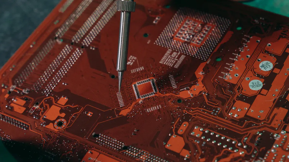
Visual and Automated Inspections
Checking for mistakes is very important in PCB assembly. It helps catch and fix problems before moving to the next step. You can use visual checks or machines, depending on your needs and budget.
Visual checks mean trained workers look for issues like bad soldering, misplaced parts, or missing pieces. This gives quick feedback to fix problems fast. But for big production, relying only on people isn’t practical because it takes time and mistakes can happen.
Machines like AOI and X-ray inspections are faster and more accurate. AOI uses cameras to spot problems like wrong solder joints or misplaced parts. X-rays are great for finding hidden issues like cracks or voids in solder.
Here’s how both methods work together:
Machines like AOI and X-ray are precise and fast, perfect for large production.
Today, AOI is the best way to find many types of defects. It’s cost-effective and ensures good quality in PCB assembly.
Note: Use both visual and machine checks for the best results. This improves quality and reduces the chance of missed defects.
Testing and Quality Control in the PCBA Manufacturing Process
Automated Optical Inspection (AOI)
AOI is important for checking the quality of PCBAs. It uses cameras to find problems like misplaced parts or bad soldering. Unlike people, AOI gives accurate results every time.
Benefits of AOI include:
It finds problems early, saving money on repairs.
It ensures every PCBA meets high-quality standards.
It reduces time and labor by automating inspections.
Evidence Type | Description |
|---|---|
Defect Detection | AOI helps spot and fix production issues quickly. |
Consistency in Inspection | Automated checks ensure all products meet strict standards. |
Cost Savings | Early problem detection lowers repair costs and saves labor. |
Adding AOI to your process improves efficiency and product quality.
X-Ray Inspection for Hidden Defects
X-Ray inspection finds hidden problems in PCBAs. It looks inside layers and connections that you can’t see. This method is great for spotting cracks, voids, or misaligned parts.
Why use X-Ray inspection?
It finds hidden issues without damaging the PCBA.
It gives detailed views of internal layers for better checks.
Inspection Method | Strengths | Limitations |
|---|---|---|
Visual Inspection | Easy and common | Only finds surface problems |
Automated Optical Inspection (AOI) | Can’t see inside layers | |
Cross-Sectioning | Shows inside details | Destroys the PCBA and takes time |
X-Ray Inspection | Finds hidden flaws without damage | Needs special tools |
Using X-Ray inspection ensures even complex PCBAs meet high standards.
Functional Testing and Validation
Functional testing checks if the PCBA works as it should. It tests the board in real-world conditions to ensure safety and reliability.
Why functional testing matters:
It finds problems early, reducing repairs and returns.
It ensures products are safe and meet customer needs.
It improves production quality and boosts profits.
It makes sure products work well, keeping customers happy.
Including functional testing helps deliver reliable and high-quality PCBAs.
Final Steps in the PCBA Manufacturing Process
Cleaning and Removing Flux Residues
Cleaning is an important part of making PCBAs. It removes leftover flux and dirt from the board. If not cleaned, these can cause rust, electrical problems, or weak solder joints.
Several things affect how cleaning is done:
The type of flux changes how easy it is to clean. R, RA, and RMA fluxes are simpler to clean, but no-clean fluxes need more work.
Flux with more solids takes longer and needs more scrubbing.
Thick flux layers under parts are harder to clean.
High heat during soldering can make residues stick to the board.
Lead-free soldering often needs stronger cleaning because of active fluxes.
Waiting too long after soldering makes cleaning tougher.
To clean well, use methods that fit your board’s needs. Common ways include ultrasonic cleaning, spray cleaning, or cleaning by hand. Regular checks make sure all dirt is gone, keeping the PCBA reliable.
Packaging for Protection
Good packaging keeps PCBAs safe during storage and shipping. Without it, boards can get damaged by moisture, dust, or bumps.
Strong packaging stops problems like bending, short circuits, or uneven parts. Materials like anti-static bags, bubble wrap, and foam protect boards from static and physical harm.
Think about how packaging materials interact with the board. Bad choices can lower quality and cause problems. By using good materials and following best practices, you can keep the board safe until it arrives.
Shipping and Delivery to Customers
The last step in making PCBAs is sending them to customers. This step needs careful planning to keep the boards safe during travel.
Pick trusted shipping companies that know how to handle electronics. Labels like “Fragile” or “Handle with Care” help avoid damage. Tracking systems let you watch the shipment and ensure it arrives on time.
By using safe packaging and good shipping plans, you can deliver high-quality PCBAs. This final step completes the process, from design to delivery, ensuring customer satisfaction.
The PCBA manufacturing process has many important steps. These include design, making the board, putting parts on it, and testing. Each step helps make strong and high-quality PCBAs. For instance, adding solder paste and reflow soldering join parts well. Checks like AOI and X-ray find problems early. These steps lower mistakes and make products work better. Industries like cars and electronics saw fewer defects after using these checks.
PCBs are key in today’s gadgets. People want smaller and stronger devices, leading to new ideas like flexible boards and dense designs. Technologies like 5G, IoT, and AI need better PCBs. These help improve phones, medical tools, and communication systems. Learning the PCBA manufacturing process helps you build new technologies for the future.
Note: Every step in the PCBA manufacturing process is needed to make strong and useful electronics.
FAQ
What is the difference between PCB and PCBA?
A PCB is just a plain circuit board. A PCBA has all the parts attached and is ready to use in devices.
Why is solder paste important in PCBA?
Solder paste helps parts stick to the board. It also creates strong electrical links during the reflow process when heat melts the paste.
How does AOI improve PCBA quality?
AOI uses cameras to find mistakes like misplaced parts or bad soldering. It catches problems early, saves money, and makes the PCBA more reliable.
What is the purpose of surface finishing in PCB manufacturing?
Surface finishing stops copper from rusting and makes soldering easier. It also helps the board last longer and work well in different conditions.
Can you reuse components from a defective PCBA?
Yes, you can reuse parts if they are not damaged. Use desoldering tools and handle them carefully to save money and reduce waste.
Tip: Check reused parts for damage before using them again.
See Also
An In-Depth Overview of PCBA Production Procedures
Key Phases Involved in the PCBA Production Process
Understanding PCBA Assembly and Its Essential Steps