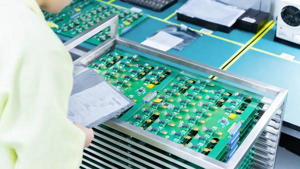
You make a printed circuit board through several key steps in printed circuit boards manufacturing. These steps transform a design into a finished product. Every stage, from design to inspection, impacts the quality and performance of the PCB. Understanding the types of PCBs and their components helps explain why each step is crucial. The printed circuit boards manufacturing process typically involves eight or nine main steps: design, imaging, etching, inspection, coating, lamination, drilling, and metallization. Each step must be performed carefully to ensure the printed circuit boards meet industry standards.
Key Takeaways
Printed circuit boards have many types and materials. Each type is picked for what the device needs. Some need to bend, handle heat, or be small.
The PCB manufacturing process has many careful steps. These steps are design, imaging, etching, drilling, plating, and finishing. They help make a strong and good board.
Quality checks happen at every step. They help find mistakes early. This stops problems and makes sure the PCB works well.
Protective layers like solder masks and surface finishes protect the board. They stop damage and help make assembly easier.
Good packaging and a final check keep PCBs safe when shipped. This makes sure they are high quality before use.
Printed Circuit Board Basics
PCB Types
There are different printed circuit boards in electronics. Each type has a special job. This changes how the circuit board works. The table below lists the main PCB types, their features, and where you might find them:
PCB Type | Description | Common Consumer Electronics Applications |
|---|---|---|
Single Sided PCB | Has metal on one side only; costs less | Calculators, radios, printers |
Double Sided PCB | Has metal on both sides; parts can go on both sides | Used more in factories and cars, not much in home devices |
Multi-layer PCB | Has many metal layers with insulation; good for hard designs | Computer motherboards, graphics cards, storage devices |
Rigid PCB | Made from hard material; can be single, double, or multilayer | Laptops, smartphones, gaming consoles |
Flexible PCB | Made from bendy plastic; can bend without breaking | Wearable devices like smartwatches, foldable smartphones |
Rigid-Flex PCB | Mix of hard and bendy layers for tricky designs | Smartphones, cameras |
You see rigid PCBs a lot in laptops and game consoles. Flexible and rigid-flex PCBs are in things that need to bend, like smartwatches. Multi-layer boards fit more circuits in small spaces.
Key Materials
Printed circuit boards use special materials for strength and performance. The most common one is FR-4. FR-4 is strong and keeps electricity safe. Polyimide is another material. It bends and handles heat well, so it is used in flexible PCBs. Teflon, also called PTFE, is good for high-frequency circuits. It does not let chemicals hurt it and has a low dielectric constant. Metal-core PCBs use aluminum or copper. These help move heat away in powerful devices. Rogers materials are used for advanced boards because they work well with electricity. You pick the material based on what the board needs to do, like handle heat, bend, or carry fast signals.
Main Components
Every printed circuit board has important parts. These parts make the circuit work. Most PCBs have these main components:
Resistors: Slow down current and turn extra energy into heat.
Capacitors: Hold and let go of electric charge when needed.
Inductors: Store energy in magnetic fields and help clean signals.
Transistors: Turn signals on and off or make them stronger.
Diodes: Let current go one way only.
Sensors: Notice changes around them and send signals.
Transformers: Move electricity between different parts of the circuit.
Tip: You will also see copper traces, solder masks, and silkscreen labels on printed circuit boards. These help connect parts, protect the board, and show where each part goes.
Now you know more about PCBs, their types, materials, and main parts. This helps you understand why each step in making them is important.
PCB Manufacturing Process Overview

The pcb manufacturing process turns your pcb design into a real board. You begin with design files and finish with a pcb you can use. The steps include cutting panels, imaging layers, and etching copper. You also drill holes, plate, and add solder masks. Legends get printed, surfaces are finished, and boards are tested. At the end, boards are separated. Each step builds on the one before it. This makes sure your printed circuit boards work well.
Pre-Production Engineering
Pre-production engineering is the first step in making a pcb. This step checks if your design data is complete and correct. Engineers look at Gerber files and BOMs to check every detail. They do a DFM analysis to see if your pcb design fits the factory’s tools. Material prep and process planning happen now. This gets copper, prepreg, and chemicals ready for use. Production drawings and process cards help workers follow each step. These tools help track progress and keep quality high. CAM files are changed to work better with machines. This stops problems like board warping. These actions lower mistakes, make pcb production faster, and help your printed circuit boards turn out better.
Note: Pre-production engineering helps your circuit board manufacturing go smoothly. You can avoid delays and big mistakes by finding problems early.
Design Review
Design review is an important part of making a pcb. You check where each part goes to make sure it is right. You look at decoupling capacitors and resistor values to see if they fit your board’s needs. Power and ground connections are checked for good signals. You run DRCs to find layout mistakes and check if the board can be made. Test plans and workflows get your pcb ready for smooth building and assembly. This step helps you find problems before they reach the factory. It saves time and money.
Tip: A careful design review makes your pcb more reliable and helps the pcb fabrication process go faster.
How long pcb manufacturing takes depends on your pcb’s type and how hard it is to make. Simple rigid boards can be made in one day and put together in another day. Harder multilayer or rigid-flex boards can take up to eleven days for everything. Things like lamination cycles, surface finishes, and getting parts can change how long pcb production takes.
Printed Circuit Boards Manufacturing Steps
When making printed circuit boards, you follow many careful steps. Each step helps shape the final pcb. These steps make sure your board works right. Let’s look at how a copper sheet turns into a multi-layer pcb.
Inner Layer Imaging
The first step is inner layer imaging. This step makes the circuit patterns inside your multi-layer pcb. You clean and roughen the copper surface first. This helps the photoresist stick better. Next, you put on a liquid photoresist and cure it. You use special phototools and UV light to show the pattern. After this, you develop the resist to see the circuit design. The copper that is not covered will be removed later.
You need special machines like contact printers and conveyorized developers. You check the quality at every step. You look for problems in the base material and photoresist. You also check the image size, spacing, and cleanliness. AOI systems help you find shorts, opens, or pattern mistakes. You keep the layers lined up very closely, less than 5 mils apart. This makes sure all layers match up in your multi-layer pcb.
Tip: Be gentle with each layer. Dust and static can ruin the imaging step.
Etching and Stripping
After imaging, you do etching and stripping. Here, you take away extra copper from the inner layers. Photoresist protects the parts you want to keep. You shine UV light to harden the resist over the pattern. Then, you wash away the soft resist. Now, the bare copper is ready to be etched.
You dip the board in an etchant solution, like ferric chloride. The chemicals eat away the exposed copper. Only the protected traces stay. You rinse the board and remove the last photoresist with solvents. This shows the finished copper traces for your circuit.
You can use acidic or alkaline solutions for etching. Acidic etching is used for inner layers. Alkaline etching is good for fast production. Some factories use dry etching with plasma for special jobs. Stripping may use strong nitric acid to take off metal layers without hurting the copper.
Inspection and Punching
After etching, you check the layers for problems. You use magnifiers and AOI systems to look for shorts or opens. FMEA helps you find and fix risks early. This stops big mistakes later.
You do visual checks at different times. You also use FCT jigs to test the circuit. During punching, you make holes in each layer. These holes help line up all the layers during lamination. IPQC checks help catch problems before assembly. This step cuts waste and makes your printed circuit boards more reliable.
Note: Careful checking now lowers the chance of problems in the final pcb.
Oxide Coating and Lamination
Now, you get the layers ready for lamination. You put an oxide coating on the copper. This makes the copper rough and helps the resin stick better. The oxide process gives more surface area and stronger bonds. This helps stop delamination in your multi-layer pcb.
Source | Role of Oxide Coating in Lamination Process |
|---|---|
PCBWay Blog | Oxide coating roughens and passivates copper, increasing resin interaction area and bond strength. |
PCBUnlimited Engineering | Oxide process alters copper surface topography to increase bond strength of prepreg to copper. |
AllPCB Blog | Oxide treatment roughens copper surface for better adhesion, preventing delamination in multilayer lamination. |
After oxide coating, you stack the layers with prepreg and copper foil. You press the stack with heat and pressure. The resin melts and bonds all the layers together. You get a solid multi-layer pcb with strong inside connections.
Drilling and Layer Alignment
Next, you drill holes through the laminated pcb. These holes connect the layers and let you add parts. Computer-controlled drills make sure holes are in the right place. The holes must be the right size and in the right spot. You keep hole placement within ±0.18 mm for good connections.
You also check that all layers line up. You use AOI and X-ray imaging to check alignment. IPC-2222 standards tell you how close the layers must be. Laser drilling is used for very small or exact holes in advanced designs.
Tip: Drilling and alignment must be accurate. This stops shorts, opens, and signal problems.
Plating and Copper Deposition
After drilling, you make the holes conductive. You do this by plating the holes with copper. First, you use electroless copper plating to put a thin copper layer inside the holes and on the surface. Then, you use electrolytic plating to make the copper thicker.
You watch the temperature, pH, and current to control copper. You check copper thickness by weighing samples before and after. Micro-etching gets the surface ready for good sticking. You check thickness and look for defects. These checks stop pinholes, uneven plating, or bad sticking.
This step is very important for your pcb. Good copper plating gives strong electrical connections between layers in your multi-layer pcb.
Note: Even copper plating is needed for a reliable printed circuit board.
PCB Surface Finishing and Testing
Solder Mask and Legend
You protect your pcb with a solder mask. This layer is green or another color. It covers the copper traces on the board. The solder mask stops solder from sticking in the wrong places. It keeps your pcb safe from water and dust. It helps prevent short circuits when you put parts on. You must put the solder mask on carefully. If it is too thick or thin, parts may not sit right. Sometimes, the mask can move under pads and cause problems. You might see issues like open circuits or tombstoning if the mask is not good. If the solder mask is thinner than 76 µm, it can break and cause trouble. Even small mistakes in placing the mask can make it hard to use tiny parts.
You also add a legend to your pcb. This is white ink printed on the board. It shows part numbers, logos, and symbols. If you put legend ink too close to small parts, it can cause problems. Ink under parts can make them rock or not sit flat. You should keep markings at least 0.15 mm away from tiny pads. In tight spaces, you may need to skip the legend.
Defect | Description | Common Causes |
|---|---|---|
Solder flows between close pads and causes shorts. | Too much solder paste, leftover flux, not cleaning after soldering. | |
Pinholes | Small holes in the solder mask show copper underneath. | Dirt during application, not enough curing. |
Peeling/Delamination | Solder mask comes off the board surface. | Bad surface prep, wrong materials. |
Missing Solder Mask | Some spots have no solder mask, so copper shows. | Problems during application like blocked stencils. |
Surface Finish
After the solder mask, you add a surface finish. This finish protects the copper that is not covered. It helps with soldering parts onto the pcb. The right finish makes your pcb last longer and work better. There are different finishes you can pick for your pcb. Each finish has good and bad points.
Surface Finish Method | Advantages | Disadvantages |
|---|---|---|
Cheap, easy to find, can be fixed, lasts long | Not flat, not good for tiny parts, has lead (HASL), can get too hot, solder can bridge, holes can get blocked | |
Immersion Tin | Flat, no lead, can be fixed, good for press fit pins | Easy to damage, uses a harmful chemical, can rust, tin whiskers, not good for many reflows, hard to measure thickness |
Immersion Silver | Flatter than HASL, better for the environment, lasts as long as HASL, cheaper than ENIG | Must solder soon after storage, can tarnish, not as strong as ENIG (no nickel) |
OSP | Flat, no lead, easy process, can be fixed, cheap | Can’t measure thickness, not good for plated holes, short shelf life, can cause testing problems, easy to damage |
ENIG | Flat, no lead, good for plated holes, lasts long | Costs more, can’t be fixed, risk of black pad, signal loss at high frequencies, hard process |
ENEPIG | Very flat, no lead, good for many assemblies, strong solder joints, can bond wires, no rust, lasts long, no black pad risk | Costs more, can’t be fixed much, some limits in processing |
Hard Gold | Tough, lasts long, no lead, lasts long | Very costly, takes a lot of work, can’t solder above 17 μin, hard to use with other finishes, risk of etching undercut |
You pick the finish based on what your pcb needs. HASL is good for most boards. ENIG is best for tiny parts. OSP is cheap for simple boards. Each finish helps your pcb handle soldering and storage.
Electrical Testing
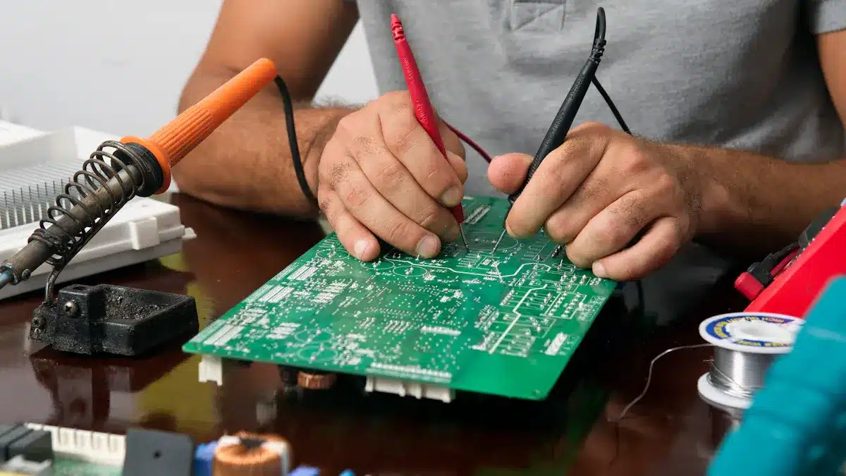
You must test your pcb before finishing it. Testing checks if every layer and connection works right. First, you look at the board to find missing parts or mistakes. AOI uses cameras to spot bad soldering or misplaced parts. ICT checks each part and connection with a special fixture. Flying probe testing uses robots to test connections without custom tools. This is good for flexible or test boards.
You may do a continuity test to make sure all connections are complete. An isolation test checks for shorts by using high voltage. Some pcbs need a functional test to see if the whole board works. You might use X-ray to check hidden solder joints. Hi-pot testing checks insulation. These steps help you find problems early and make sure your pcb is good.
Tip: Careful testing at every step helps you avoid big mistakes and makes sure your pcb works in real life.
Final PCB Assembly and Quality

Depaneling
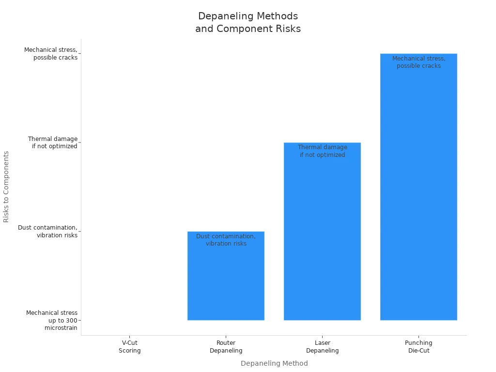
Depaneling is when you take finished boards off a big panel. In big factories, machines do this job fast and safely. Each depaneling way has good and bad points. The table below shows how each method works and what to watch for:
Method | Description | Pros | Cons | Risks to Components | Best Use Case |
|---|---|---|---|---|---|
V-Cut Scoring | Machine makes V-shaped lines; boards are snapped apart by hand or tool. | Cheap, quick, good for straight cuts | Can stress edges | Stress at edges, may hurt parts | Medium batches, rectangle boards |
Router Depaneling | CNC machine uses a spinning bit to cut tabs or links. | Very exact, good for odd shapes | Slower, makes dust, costs more | Dust, shaking can hurt parts | Odd shapes, small to medium batches |
Laser Depaneling | Laser beam cuts boards with great accuracy, no touching. | No stress, very clean cuts | Expensive, slow for thick boards | Heat can hurt parts if not careful | Fancy, high-precision boards |
Punching / Die-Cut | Special die punches out boards from the panel in one press. | Super fast, always the same | Tools cost a lot, can stress boards | Stress, cracks can happen | Big batches of simple, same-shape boards |

Punching and V-cut scoring are good for lots of boards but can hurt the edges. Laser depaneling makes smooth cuts and less stress, but heat must be controlled. Always pick the best way for your pcb so your parts stay safe.
Final Inspection
You must check every pcb before it leaves the factory. Final inspection makes sure your pcb is good quality. You use many tools and tests to find problems:
Look for bad solder, cracks, scratches, or lifted leads.
AOI checks your pcb against a perfect one to find missing or wrong parts.
X-ray finds hidden problems like empty spots or cracks inside.
ICT tests if each part and wire works right.
Functional testing turns on the pcb to see if it works.
Magnifiers, microscopes, and cameras help you see tiny problems.
You need to make sure your pcb matches the plan, has no mistakes, and works well. This step is very important for making good pcbs.
Tip: Good factories follow IPC, ISO, and UL rules to make sure every pcb is safe and high quality.
Packaging
You keep your pcb safe during shipping and storage by packing it well. Always wear gloves or finger covers so you do not get dirt on the board. Use both hands to pick up the pcb and keep it flat. Store boards in closed boxes with drying packs to stop water. ESD-safe bags and boxes keep away static.
Here are some ways to pack pcbs:
Black plastic boxes that block static
Anti-static foam shipping boxes
Bubble mailers that block water and static
Bags that block water and vacuum-sealed packs
Stiffeners for thin or bendy boards
Soft stuff like Styrofoam in boxes
Label each box with part numbers and dates. Keep the storage place cool and dry. Always use the oldest boards first so none sit too long. Do not open the package until you need the pcb for assembly.
Note: Packing and storing your pcb the right way keeps it safe from harm, water, and static, so it is ready when you need it.
You have seen how each step in the pcb process builds a reliable board.
You start with careful design and material selection to meet your needs.
You use imaging and etching to protect copper traces and keep signals strong.
Lamination, drilling, and plating give your pcb solid connections.
Solder mask, surface finish, and clear labels help with assembly and durability.
Testing and inspection catch problems early.
Every process step uses precision and quality checks to stop defects. When you understand these steps, you see the skill and care needed in pcb production. If you want to learn more, look for resources on advanced techniques, assembly methods, and industry standards.
FAQ
What is the most common material used for PCBs?
You will find FR-4 as the most common material. FR-4 is a strong fiberglass material. It keeps your board safe from heat and electricity. You can use it for most consumer electronics.
How do you choose the right PCB type for your project?
You should look at your project’s needs. If you need a simple board, use a single-sided PCB. For complex devices, pick a multi-layer or rigid-flex PCB. Think about size, flexibility, and how much power your board needs.
Why do you need a solder mask on a PCB?
A solder mask protects your board’s copper traces. It stops solder from sticking where it should not. You also keep your board safe from dust, water, and short circuits. Solder masks help your board last longer.
How do you test if a PCB works before using it?
You can use electrical tests. These tests check for open circuits and shorts. Automated Optical Inspection (AOI) finds missing or misplaced parts. Some factories use X-ray or functional tests to make sure your board works right.
See Also
Key Stages Involved In The PCBA Production Process
Detailed Walkthrough Of The PCBA Manufacturing Procedure
Complete Overview Of Essential PCBA Production Steps