Measuring the process measurement PCB assembly steps helps devices work well and stay reliable. Mistakes during the process measurement PCB assembly can cause problems, cost more money, and lose customer trust. Testing is important to stop these problems.
Mistakes can make devices stop working or work poorly.
Bad assemblies waste materials, need fixing, or may be recalled, raising costs.
Regular testing and keeping records make devices better and ensure quality.
Using tools like automated tests and step-by-step methods helps check processes and make great process measurement PCB assemblies.
Key Takeaways
Testing often during PCB assembly avoids big mistakes and ensures products work well.
Using tools like X-ray machines and auto inspections makes solder joints better and lowers errors.
Placing parts correctly is important; check machines often to keep them precise and avoid mistakes.
Use stress tests to find weak spots in PCBs and make them last longer in hard conditions.
Checking inspection data shows patterns, improves steps, and keeps PCB quality high.
Key Metrics for Process Measurement in PCB Assembly
Knowing the main metrics in PCB assembly helps ensure good results. These metrics check how well your assembly works and show areas to improve. Let’s look at the most important ones.
Solder Joint Quality
Solder joints attach parts to the PCB, so their quality matters. Bad solder joints can cause device failures, shorter lifespans, or complete breakdowns. Checking solder joint quality means looking at strength, evenness, and no cracks or gaps.
Better methods can greatly improve solder joints. Slice analysis shows inside structures to find tiny problems. Scanning acoustic microscopy spots hidden issues like cracks. Infrared analysis finds dirt that affects soldering. These tools help make solder joints top-notch.
Technique | What It Does |
|---|---|
Slice Analysis | Shows inside PCB layers to find small defects and improve quality. |
Scanning Acoustic Microscopy | Finds hidden problems like cracks without damaging the PCB. |
Microscopic Infrared Analysis | Spots dirt that makes soldering harder, helping fix process issues. |
Scanning Electron Microscopy | Gives detailed images of surfaces and materials, useful for fixing failures. |
Using these tools makes solder joints better and lowers the chance of problems in your assembly.
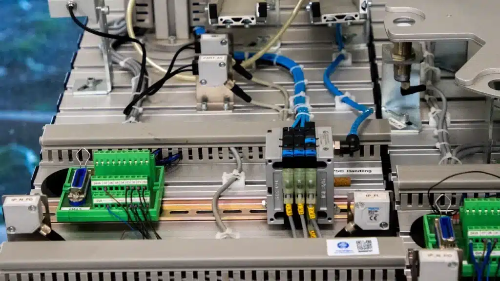
Component Placement Accuracy
Placing parts correctly ensures the PCB works as it should. Misplaced parts can cause errors, signal problems, or stress on the board. Checking placement accuracy means seeing how close parts are to their spots.
The machine capability index (cmk) measures placement precision. A cmk of 1.33 means fewer mistakes, while 2.66 means even better accuracy. For example, with 75 μm placement accuracy, a cmk of 1.45 leads to fewer than 60 errors per million placements. This precision reduces mistakes and improves assembly performance.
To get better placement accuracy, use advanced machines and calibrate them often. These steps keep your assembly consistent and increase success rates.
Electrical Functionality
Electrical testing checks if the PCB works without problems. This metric tests if circuits send signals correctly and keep voltage steady. Bad electrical function can cause device failures or unsafe use.
Tools like multimeters and oscilloscopes measure electrical performance. They check voltage, current, and signal quality. Test fixtures mimic real-world use to find and fix problems early.
Regular electrical testing ensures reliable products and avoids costly recalls. Adding this metric to your PCB assembly process helps meet customer needs and industry rules.
Thermal Performance
Thermal performance is key to keeping your PCB assembly reliable. Too much heat can harm parts, weaken materials, and shorten product life. Checking how your PCB handles heat helps find problems early.
You can measure thermal performance using different metrics. These metrics show how heat changes the electrical, mechanical, and structural parts of your PCB. The table below explains common methods:
Metric Type | Description |
|---|---|
Electrical Performance | Check resistance, capacitance, and impedance changes under heat stress. |
Mechanical Properties | Test strength, flexibility, and how well parts stick together. |
Microstructural Analysis | Use tools like SEM and XRD to study material changes from heat. |
Watching these metrics ensures your PCB stays strong in tough conditions. For example, microstructural analysis shows damage from repeated heating and cooling. This helps you improve your design or pick better materials.
Tip: Use thermal cameras or infrared sensors to see heat spots on your PCB. This helps you fix hot areas and improve heat flow.
Adding thermal performance checks to your process measurement PCB assembly makes your product tougher. It also boosts reliability and keeps customers happy.
Signal Integrity
Signal integrity makes sure your PCB sends data correctly and quickly. Bad signals can cause errors, slow speeds, or system failures. Testing signal integrity helps fix problems that could hurt your product.
Many things affect signal integrity, like impedance, delay, and crosstalk. The table below lists these factors and their effects:
Factor | Description |
|---|---|
Impedance | Changes cause signal reflections and distortions, lowering quality. |
Propagation Delay | Timing issues lead to errors, especially with fast signals. |
Attenuation | Signals weaken due to trace resistance, worse at high speeds. |
Crosstalk | Nearby traces cause interference, leading to data mistakes. |
Ground Bounce | Voltage shifts in the ground can mess up signals. |
Supply Voltage Fluctuations | Voltage drops during switching create noise and errors. |
Electromagnetic Interference | Noise from switching can badly affect signal quality. |
To keep signals clear, fix these issues during design and testing. Here’s how:
Match impedance to stop signal reflections.
Use shorter traces to avoid delays.
Add shielding to block crosstalk and interference.
Note: High-speed PCBs face more signal problems. Pay extra attention to delay and signal weakening.
By solving these problems, your PCB will work better. Signal integrity testing is a must for process measurement PCB assembly. It ensures your product meets standards and satisfies customers.
Tools and Techniques for PCB Assembly Testing
Testing tools are important for making sure PCBs work well. Using advanced tools helps find problems early, improve performance, and save money. Below are some key tools and methods to know.
Automated Optical Inspection (AOI) Systems
AOI systems use cameras to check PCBs for visible problems. They can spot issues like bad soldering, missing parts, or misaligned components. AOI works fast and gives accurate results, making it great for large production runs.
Advantages of AOI | Challenges of AOI |
|---|---|
Finds visual issues quickly | Needs trained users |
Works at many stages | Can't see hidden problems |
Saves money for big batches | Costs a lot to maintain |
AOI systems help by catching mistakes early. This stops errors from happening again and keeps quality steady. For example, if a part is out of place, the system flags it so you can fix it right away.
Tip: Update AOI software often to handle new PCB designs and improve detection.
X-Ray Inspection Machines
X-ray machines find hidden problems in PCBs. They show defects like solder gaps, inside misalignments, and not enough solder. This method checks the board without causing damage.
Soldering Defects | Found by X-Ray |
|---|---|
Solder gaps | Yes |
Inside misalignments | Yes |
Not enough solder | Yes |
X-ray tools are great for complex PCBs with many layers. They help catch problems early, saving time and money. For instance, finding a solder gap during testing lets you fix it before shipping the board.
Note: X-ray machines are expensive but worth it for critical or high-value projects.
Multimeters and Oscilloscopes
Multimeters and oscilloscopes test how well PCBs work electrically. Multimeters measure voltage, current, and resistance. Oscilloscopes show signal patterns. Together, they check if the PCB works as it should.
Good probes make these tools more accurate. Probes with gold tips give better readings by lowering contact resistance. Bad probes can mess up signals and give wrong results.
Tip: Use multimeters for simple tests and oscilloscopes for detailed signal checks. This combo ensures your PCB's electrical performance is tested thoroughly.
Adding these tools to your PCB assembly process improves reliability and meets industry standards.
Functional Test Fixtures
Functional test fixtures are tools that check if your PCB assemblies work properly. They mimic real-life conditions to test the boards before they leave the factory. These tools help find problems, confirm performance, and ensure the boards meet industry rules.
The table below shows how functional testing improves PCB performance:
Evidence Description | Impact on PCB Functionality |
|---|---|
Boards that pass tests are higher quality and last longer, making customers happier. | |
Testing ensures boards follow safety and quality rules. | Confirms that PCBs meet important standards needed for electronics. |
Finding problems helps improve designs and processes. | Makes future production better, faster, and less expensive. |
Virtual testing checks 50-100% of boards before shipping. | Ensures most boards are tested and working before reaching customers. |
Skilled testers make testing faster and more effective. | Lowers the chance of defects, so products leave the factory in great shape. |
Functional test fixtures improve PCB quality and save time and money by catching issues early. Adding this step to your process ensures your products meet customer needs and follow regulations.
Environmental Stress Testing Chambers
Environmental stress testing chambers check how PCBs handle tough conditions. These chambers copy real-world environments to find weak spots in your designs.
Here are some key tests done in these chambers:
Humidity testing – Checks if the board can handle damp air.
Salt spray testing – Tests durability in salty environments, like near oceans.
Thermal shock – Quickly switches between hot and cold to test coatings’ strength.
Temperature chambers are especially useful for testing real-use conditions. They can quickly change or hold environmental factors like heat or humidity. This helps see how PCBs perform under stress, such as extreme temperatures or moisture.
Using environmental stress testing chambers ensures your PCBs stay strong in harsh conditions. This step improves product quality and builds customer trust in your designs.
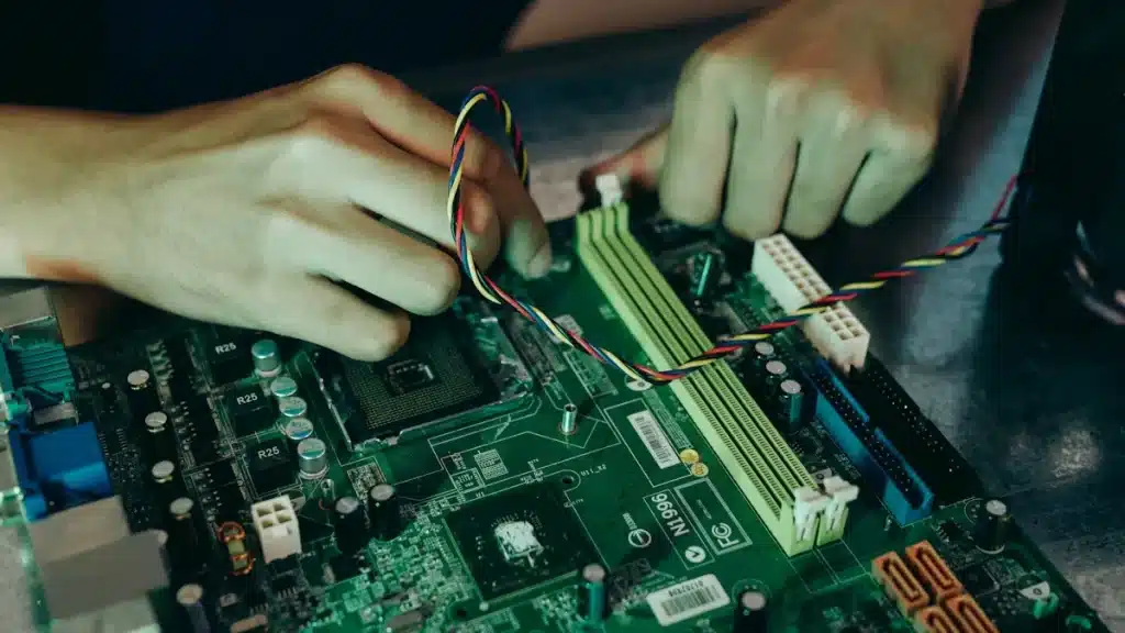
Step-by-Step Process Measurement for PCB Assembly
Conducting Visual Inspections
Visual checks are the first step to ensure PCB quality. This means looking for visible problems like misplaced parts, bad soldering, or broken traces. Finding these issues early can stop bigger problems later.
To do visual checks well:
Use tools like magnifying glasses to see small problems.
Look for smooth solder joints without cracks or gaps.
Make sure all parts are in the right place and direction.
Visual checks are most helpful at the start of assembly. For example, checking the etching process ensures pathways are clean and accurate. This step affects how well the final product works.
Step | What Happens |
|---|---|
1 | Etching: Removes extra copper to create clear pathways. |
2 | Component Mounting: Places parts using SMT or THT methods. |
3 | Soldering: Connects parts with manual or reflow soldering. |
4 | Quality Check: Finds issues using visual, AOI, or X-ray inspections. |
5 | Final Assembly: Combines PCB with other parts for full use. |
6 | Testing: Checks performance under different conditions. |
Visual checks are key to catching mistakes early. This saves time and materials.
Performing Functional Testing
Functional testing makes sure the PCB works as it should. It copies real-life conditions to check the whole assembly. This helps find and fix problems before customers get the product.
Benefits of functional testing include:
Testing how the PCB works in real situations.
Checking if all parts work together properly.
Finding problems like power issues or signal errors.
Functional testing lowers the chance of PCB failures. For example, PCBs with this testing fail only 0.0003% of the time, compared to 0.03% without it.
Testing Method | Failure Rate |
|---|---|
With Functional Testing | 0.0003% |
Without Functional Testing | 0.03% |
Functional test tools are very important. They copy real-world use and let you test all products before shipping. This ensures your PCBs meet rules and customer needs.
Tip: Use skilled workers and good tools to make functional testing better and faster.
Utilizing Environmental Stress Testing
Environmental stress testing checks how PCBs handle tough conditions. This step finds weak spots and makes products stronger.
Common tests include:
Humidity testing: Checks if the board can handle wet air.
Thermal shock: Tests how it reacts to quick temperature changes.
Salt spray testing: Sees if it lasts in salty environments.
Stress testing is great for finding solder joint problems caused by stress. For instance, lead-free solder can crack more easily under pressure. Strain gage testing shows where stress is highest, helping improve designs.
Evidence Description | Key Insights |
|---|---|
Stress can cause solder joints to fail in PCBs. | Shows why stress testing is needed to find weak spots. |
Strain gage testing finds high-stress areas and bad designs. | Helps fix designs to avoid future problems. |
Stress tests copy real-life conditions for PCBs. | Proves stress testing is useful for checking PCB reliability. |
Adding stress testing to your process ensures your PCBs stay strong in harsh conditions. This step improves quality and builds customer trust.
Understanding Data from Inspection Tools
Inspection tools collect a lot of data during PCB assembly. Looking at this data helps find patterns, fix problems early, and make production better. By using smart methods, you can turn raw data into useful information.
One helpful way is to use machine learning for analysis. For example, the XGBoost method improves maintenance systems. It spots changes in temperature curves to find issues. This method predicts failures with high accuracy. Fixing problems early keeps quality steady and reduces downtime. It also makes the PCB assembly process smoother and more efficient.
To use inspection data well, follow these steps:
Gather Data Regularly: Make sure tools like AOI and X-ray machines work properly.
Show Data Clearly: Use charts to spot patterns or unusual results in solder joints or part placement.
Predict Problems Early: Use machine learning to find and fix issues before they happen.
Check and Improve: Review your methods often and update them when needed.
Tip: Teach your team how to read and use data from inspection tools. This helps improve the production process effectively.
Checking Results Match Design Plans
Checking test results against design plans ensures PCBs work as expected. This step confirms the product meets quality standards and works well in real-life situations.
Different tests help confirm this. The table below shows key tests and their purposes:
Test Type | What It Checks |
|---|---|
Impedance Testing | Makes sure high-speed traces match planned impedance. |
Signal Integrity Testing | Tests signal quality on fast circuits using special tools. |
Power Integrity Testing | Checks if power systems stay stable under changing loads. |
EMI/EMC Testing | Measures noise from PCBs and their resistance to outside interference. |
Environmental Stress Testing | Tests boards in tough conditions like heat, cold, and vibration. |
HASS/HALT | Finds early failures by stressing boards more than usual. |
Burn-in Testing | Runs boards under high voltage and heat to find hidden problems. |
Netlist Testing | Verifies all connections match the design. |
Resistance/Continuity Testing | Checks for proper resistance and finds broken or shorted connections. |
Insulation Resistance Testing | Measures resistance to ensure no shorts between conductors. |
High Pot Testing | Tests insulation strength with high voltage. |
Operational Life Testing | Runs boards for a long time to check for wear and tear. |
Temperature Cycling | Heats and cools boards repeatedly to test solder joint strength. |
Vibration Testing | Shakes boards to check if they can handle movement. |
Drop/Shock Testing | Drops boards to test if parts stay attached after impacts. |
These tests confirm PCBs meet both functional and environmental needs. For instance, impedance testing ensures signals stay clear, while stress testing checks durability in harsh conditions.
Note: Always compare test results to the original design plans. This helps catch problems early and fix them before making large quantities.
Optimizing PCB Assembly Testing Processes
Using Data to Improve Testing
Data analysis helps make PCB testing better. By studying test results from many production runs, you can find hidden patterns. For example, big data tools show small trends to improve designs and processes. Statistical process control (SPC) methods also help by spotting issues early. These methods let you adjust tests, focus on problem areas, and avoid extra checks.
Using data ensures fair quality checks, which are key for improvement. For instance, studying temperature changes during tests can predict failures. This early action reduces delays and makes PCB assembly more efficient.
Making Continuous Improvements
Continuous improvement keeps PCB assembly fast and reliable. Companies using this method often see big gains. For example, one company tracked production data and machine performance. This cut down on delays, reduced errors, and improved efficiency.
To start, review production data often. Find weak spots and fix them quickly. Use tools like SPC and monitoring software to track changes. Over time, small fixes add up to better quality and faster production.
Training Your Team on New Testing Methods
Your team is key to successful PCB testing. Teaching them advanced testing skills helps them use modern tools well. For example, learning to operate automated inspection systems or read X-ray data improves accuracy.
Regular training also keeps your team updated on industry rules and new methods. This boosts their skills and ensures your processes stay current with technology. A skilled team is your best resource for making high-quality PCBs.
Integrating Testing into the Production Workflow
Adding testing steps directly into production keeps quality steady. It also helps find and fix problems early, saving time and materials.
To do this, use design for testing (DFT) ideas when planning your PCB. DFT makes testing easier and improves product quality. For example:
Smart DFT methods make testing faster and less expensive.
Free functional PCBA testing shows you care about quality.
In-circuit test (ICT) systems are also important for this process. These tools check each part on the PCB to ensure accuracy. Modern ICT tools, like bed-of-nails fixtures and flying probe testers, work well with complex boards. They make sure all parts work, even in tricky designs.
By adding testing to your production steps, you improve quality and speed up delivery. This approach reduces mistakes and builds customer trust.
Tip: Check your testing methods often and update them for new PCB technologies.
Collaborating with Suppliers for Quality Assurance
Working with suppliers helps keep quality high and avoids problems. Good teamwork makes it easier to spot and fix issues early.
Studies show sharing information with suppliers improves results. For example:
One factory used a chi-square test to study soldering problems. This helped them fix issues, cut costs, and make products more reliable.
Tracking defects with tools like chi-square tests helps improve quality over time.
Research shows that working closely with suppliers and sharing goals boosts efficiency and product quality.
Strong supplier relationships ensure every PCB meets your standards. Open communication and teamwork lead to better products and happier customers.
Note: Regular checks and feedback with suppliers can improve PCB assembly quality even more.
Checking how you assemble PCBs makes sure they work well. It helps find problems early, keeps quality steady, and makes production smoother. Some key benefits are:
Doing each step right to make ready-to-use circuit boards.
Faster assembly with tools like feeders and placement machines.
Keeping boards clean, no matter the design.
Final tests that find mistakes before shipping.
Using simple designs to make building easier.
Improving testing methods makes products even more reliable. For instance, having ISO 9001:2015 shows you care about quality. Using better tools and training workers ensures good testing. Updating your methods often lowers mistakes, makes products work better, and keeps customers happy.
By using these ideas, you can make better PCBs that people trust. Keep improving to stay ahead in the busy electronics market.
FAQ
What is the most important metric to measure in PCB assembly?
Solder joint quality is very important. It keeps parts firmly attached and working well. Bad solder joints can cause devices to fail or not last long. Regular checks with tools like X-ray machines or scanning electron microscopes help keep quality high.
How often should you perform functional testing during PCB assembly?
You should test at several points during assembly. Testing early finds problems before they get worse. Final testing makes sure the PCB works as planned and meets design needs.
Can environmental stress testing damage PCBs?
Stress testing does not harm well-made PCBs. It copies tough conditions to find weak spots. If a PCB fails, it shows where to improve. This testing ensures your product works well in hard environments.
What tools are best for detecting hidden defects in PCBs?
X-ray machines are great for spotting hidden problems like solder gaps or misaligned parts. They give clear images without harming the PCB. Advanced tools like scanning acoustic microscopes can also find cracks or layers coming apart.
How can you improve signal integrity in high-speed PCBs?
To improve signal integrity, match impedance, use shorter traces, and add shielding. These steps stop signal problems like delays or interference. Tools like oscilloscopes and signal analyzers check if your PCB works properly.
Tip: Always check your PCB design for signal issues before making it.