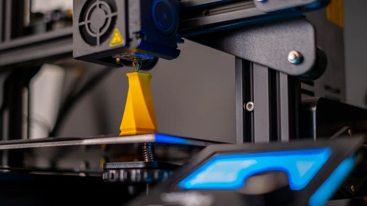
3D printing has revolutionized the process of prototyping PCBA with 3D printing, making it faster and more cost-effective than ever before. As electronics become increasingly complex, the demand for quick prototyping is essential. 3D printing contributes to this need by operating very efficiently. Companies are leveraging advanced tools like AI and machine learning to enhance their designs, resulting in products that are quicker to manufacture and of higher quality.
By 2025, the integration of 3D printed circuit boards will open up new opportunities for engineers and hobbyists alike. The market for 3D printed electronics is projected to reach $263.5 million, growing rapidly at a rate of 25.2% each year. The ability to create custom designs or small prototypes has become easier and more beneficial with the advent of 3D printing technology.
Key Takeaways
3D printing helps make PCB prototypes quickly and cheaply.
It allows testing designs fast without spending too much money.
You can create custom shapes and features with 3D printing.
Traditional methods can’t easily make these unique designs.
Hobbyists can build PCBs at home with low-cost 3D printers.
This makes electronics projects easier for more people to try.
Picking the right materials and printer is very important.
It affects how strong and heat-resistant your PCB will be.
Testing and fixing problems are key to making your PCB work.
These steps ensure it meets the design rules and works well.
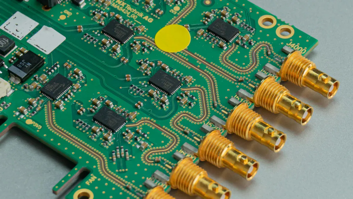
Benefits of 3D Printed Circuit Boards
Cost-effectiveness and reduced waste
3D printed circuit boards save money and cut down on waste. Regular PCB production costs a lot and wastes materials. With 3D printing, you only use the materials needed for your design. This method lowers waste and makes production cheaper. It’s great for small projects or new businesses.
Also, 3D printing doesn’t require making many copies at once. You can print one prototype or a few without spending much. This lets you try out different designs without worrying about money.
Faster production cycles for iterative design
3D printing speeds up making prototypes, so ideas come to life fast. Regular methods can take weeks, but 3D printed boards are ready in hours. This helps you test and improve designs quickly, saving time on final products.
If changes are needed, you can update the design file and print again. This quick process shortens development time and keeps you ahead in competitive markets.
Enhanced design flexibility and customization
3D printed circuit boards allow creative and flexible designs. Regular PCBs are flat and stiff, but 3D printing lets you make curved or 3D shapes. This opens up new ways to create unique designs.
You can also customize PCBs for special needs or projects. For example, you can print circuits directly onto objects for better integration. Custom designs reduce waste and improve how electronics work, making them eco-friendly and modern.
Accessibility for small-scale and hobbyist projects
3D printed circuit boards help hobbyists and small creators make prototypes. Regular PCB manufacturing needs big orders, costly tools, or outside help. These challenges often stop people or small teams from trying their ideas. With 3D printing, you can skip these problems and make PCBs at home or in a small space.
You just need a 3D printer, materials, and a design file to start. Many low-cost 3D printers today can create PCBs. This lets you test designs without spending much or waiting long. Hobbyists can use this to build personal projects like gadgets, robots, or wearable tech.
Small projects also gain from the flexible designs of 3D printed PCBs. You can make special shapes or add circuits to unique designs. For example, you could print a curved PCB to fit a case or directly onto a 3D object. Traditional methods can’t easily do this.
Online groups and guides make learning about 3D printed PCBs simple. You can find tutorials, design files, and tips from other makers. Sharing ideas helps you improve and try new things.
With 3D printing, you can test and create freely without old manufacturing limits. Whether you’re a hobbyist or small creator, this tech gives you control to invent and explore.
Step-by-Step Guide to Prototyping PCBA with 3D Printing
Picking the right 3D printer and materials
Choosing the best 3D printer and materials is key. Match your project needs with printer features and material options. Think about strength, flexibility, and heat resistance for real-world use.
Here’s a simple table to help you decide:
Feature | What It Means |
|---|---|
Strength | Makes sure your prototype lasts and works well. |
Flexibility | Needed for designs that bend or handle impacts. |
Chemical Resistance | Protects PCBs from damage caused by chemicals. |
Heat Resistance | Keeps parts safe in high-temperature conditions. |
Surface Finish | Improves how the printed parts look and work. |
Cost | Helps you pick materials within your budget. |
Tech Compatibility | Ensures the material fits your printer type. |
Post-Processing Needs | Shows if extra steps are needed after printing. |
SLA printers give smooth finishes and high detail. FDM printers are cheaper and good for basic prototypes. Materials like PLA and ABS are common, while resins work for detailed designs.
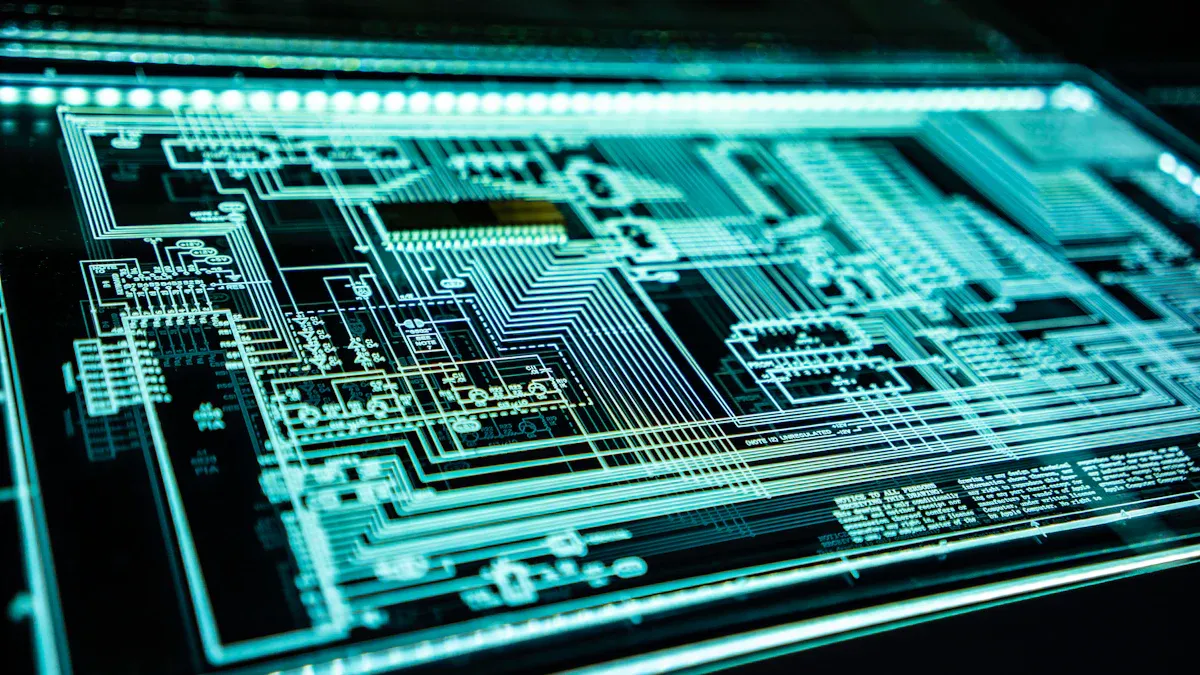
Making the PCB design file (GERBER format)
You need a PCB design file before printing. Most printers use GERBER files, which hold layout details. Use software to make or edit your design. Include trace widths, pad sizes, and layers.
Check your design for mistakes using software tools. These tools find problems like overlapping traces or wrong sizes. Fix errors early to avoid wasting time and money.
Printing the PCB prototype
Load your design file into the printer software. Adjust settings based on your printer and material. SLA printers need resin settings, while FDM printers use filament adjustments.
Printing is fast and saves money. You can make PCBs without waiting for outside help. 3D printing also lets you create custom shapes for your project.
Here’s a quick table of 3D printing benefits:
Benefit | Why It Matters |
|---|---|
No long waits like traditional methods. | |
Saves Money | Cuts costs for making PCBs. |
Flexible Designs | Allows unique shapes for special projects. |
Protects Ideas | Keeps your designs private by printing at home. |
Quick Changes | Lets you test and improve designs easily. |
After printing, check your prototype for problems. Fix any issues to make sure it works as planned.
Assembling and soldering components
After printing your PCB, the next step is assembly. This means adding and soldering parts to make it work. Gather all needed items like resistors, capacitors, ICs, and connectors. You’ll also need a soldering iron, solder wire, and tweezers for small parts.
Place each part on its correct spot on the PCB. Use your design file to check where everything goes. For tiny parts like SMDs, tweezers help you position them. If using through-hole parts, push their leads into the holes and bend them slightly to keep them steady.
When soldering, be careful and quick. Touch the soldering iron to the joint for just a few seconds. Too much heat can harm parts or the board. Use enough solder to make a shiny, small dome shape. Don’t use too much, as it can cause connections to touch by mistake.
If you want to avoid soldering, new methods are available. SolderlessPCB techniques have worked well in tests. Boards made this way stayed functional for months. They also matched soldered boards in performance, making them a good option for certain designs.
After soldering, check your work carefully. Look at the joints with a magnifying glass to find problems like weak joints or extra solder. For hidden parts, advanced tools like X-rays can help. This step ensures your PCB is ready for testing.
Testing and troubleshooting the prototype
Testing makes sure your PCB works and finds any problems. Start by looking at the board to see if parts are in the right spots. Check for damage like burnt areas or crooked parts.
Next, test the board’s connections with a multimeter. This tool checks if everything is connected and there are no short circuits. For complex boards, special tests like in-circuit or flying probe testing can check each part’s performance. These tests confirm your design works as planned.
If the board passes, test it under tough conditions. Try heat, moisture, or shaking to see if it holds up. Burn-in testing runs the board for a long time to find weak spots.
If the board fails, find and fix the problem. Common issues include broken connections, wrong part placement, or short circuits. Use tools like oscilloscopes to locate the issue. Fixing problems early saves time and ensures the board meets standards.
3D printed PCBs may have unique problems. About 20% of FDM printing issues come from user mistakes, like running out of filament or poor adhesion. Double-check your design and printer settings to avoid these errors.
Testing and fixing problems improve your PCB’s quality. Catching issues early saves money and time. This ensures your board is ready for real-world use.
Types of 3D Printing Technologies for PCBs
FDM (Fused Deposition Modeling) and its uses
FDM is a simple way to print PCBs. It builds shapes by melting plastic and stacking layers. This method is cheap and easy for small projects. Hobbyists use FDM to test PCB designs quickly.
FDM has benefits over older methods. It makes complex shapes without molds. It also speeds up testing new designs. Below is a table comparing FDM and traditional PCB methods:
Feature | FDM Printing | Traditional Methods |
|---|---|---|
Design Options | Flexible, allows unique shapes | Limited, needs molds |
Fast Prototyping | Quick, good for testing ideas | Slower, takes longer to set up |
Material Use | Moderate, uses plastic | High, optimized for specific materials |
Cost | Lower for small projects | Higher due to setup costs |
FDM isn’t perfect. It lacks precision and smooth finishes, so it’s not ideal for detailed PCBs.
SLA (Stereolithography) for detailed designs
SLA uses lasers to harden liquid resin into solid layers. It creates very detailed and smooth PCBs. This makes SLA great for designs needing high accuracy.
SLA printers can use heat-resistant resins. These resins handle soldering heat well, making them good for working prototypes. SLA costs more than FDM but offers better precision and material choices. Professionals often pick SLA for complex projects.
SLS (Selective Laser Sintering) for tough prototypes
SLS uses lasers to melt powder into strong shapes. It’s perfect for advanced PCB designs needing durable parts. SLS can add features like copper layers or antennas directly into the PCB.
SLS can make multi-layer PCBs in one step. It uses special materials to create working prototypes that feel like finished products. SLS needs special tools and skills but is great for cutting-edge designs.
Challenges in Prototyping PCBA with 3D Printing
Fixing warping and material problems
Warping happens when the board bends or twists. This occurs if the material cools unevenly. Warping can cause parts to not fit right. It also makes connections unreliable. To stop warping, keep the printing area warm and steady. Avoid cold drafts that cool the material too fast.
Picking the right materials helps too. Resins that handle high heat are better. These resins don’t warp easily and work well for soldering. They can handle temperatures over 200°C, making them great for lead-free soldering. Mixing methods, like adding copper layers, can make boards stronger.
Material problems like uneven layers can hurt your PCB’s performance. Fix this by using special techniques during printing. Methods like plasma activation or chemical vapor deposition (CVD) make layers stick better. This creates stronger and longer-lasting boards.
Stopping short circuits and improving conductivity
Short circuits happen when traces touch by mistake. This is common in 3D-printed boards with uneven surfaces. To avoid this, check your design file carefully before printing. Make sure traces have enough space between them.
Using better materials can help too. Nano-copper paste with laser sintering improves conductivity. It also lowers the chance of short circuits. After printing, add a protective layer to keep traces safe from moisture or accidental contact.
Testing is very important. Use a multimeter to check for unwanted connections. For complex boards, use 3D X-ray systems. These tools find hidden problems without damaging the board.
Making parts accurate and aligned
Parts need to be placed correctly for the PCB to work. Misaligned parts can cause bad connections or make the board fail. To fix this, focus on printing and assembly steps.
Modern printers like SLA and SLS are more precise than FDM. They make smoother surfaces and detailed designs. This helps you place parts more accurately. During assembly, tools like solder paste inspection (SPI) check solder amounts. This ensures parts stick securely.
AI can also improve accuracy. It finds mistakes and suggests better ways to place parts. Machine learning can study your design and reduce errors. Below is a table showing how different tools improve precision:
Technology/Methodology | How It Helps |
|---|---|
Finds hidden problems without damaging the board. | |
SPI Technology | Checks solder paste for correct size and shape before placing parts. |
AI Algorithms | Spots mistakes and improves part placement using smart learning. |
Using these tools makes your PCB more accurate and reliable. This ensures your prototype works well and lasts longer.
Fixing Problems with Current 3D Printing Materials
Materials for 3D printing PCBs have improved but still have issues. These problems can affect how well your prototype works. Common issues include low conductivity, poor heat resistance, and weak strength. Solving these problems is important for making reliable designs.
Common Problems with Current Materials
Low Conductivity: Most materials don’t conduct electricity as well as copper. This makes PCBs less efficient, especially for high-power uses.
Heat Issues: Many materials can’t handle the heat from soldering or use. This can cause bending or damage over time.
Weak Strength: Some materials break or bend easily under pressure. This makes them unsuitable for tough environments.
Ways to Solve These Problems
You can improve your prototype by following these steps:
Pick Better Materials: Use materials made for PCBs, like nano-copper paste or conductive resins. These materials conduct electricity better and resist heat up to 200°C, which is great for soldering.
Adjust Printer Settings: Change settings to make stronger prints. For example, improve layer bonding to avoid weak spots. Use methods like plasma activation or chemical vapor deposition (CVD) to make materials stick better.
Add Protective Coatings: After printing, apply coatings to protect the PCB. These coatings improve durability and keep moisture or accidental touches from causing problems.
Future Improvements in 3D Printing Materials
New materials are being developed to fix these issues. Future materials will conduct electricity better, handle more heat, and be stronger. These changes will help 3D-printed PCBs work as well as traditional ones.
In the future, printers will also have higher resolution and be able to add complex parts during printing. This will make it easier to create detailed PCBs with fewer limits.
Tip: Keep learning about new materials and tools. Using the latest options can make your designs better and more competitive.
By fixing today’s problems and using future advancements, you can make strong and reliable PCBs with 3D printing. This ensures your prototypes meet modern needs.
Future Trends in 3D Printed Circuit Boards
Better conductive materials for 3D printing
The future of 3D printed circuit boards depends on better conductive materials. These materials make designs work more efficiently and last longer. Conductive inks are improving quickly. By 2037, the market for these inks will grow to $5.97 billion, increasing by 4.5% each year. Most of this growth will happen in Asia Pacific, which will control 45% of the market.
In the U.S., scientists are working on new conductive materials. For example, Lawrence Livermore National Laboratory is creating advanced conductive inks for 3D printing. These new materials will make PCBs stronger and better at conducting electricity. High-temperature resins and nano-copper paste with laser sintering are already showing good results. They can handle lead-free soldering and lower electrical resistance, making them perfect for modern uses.
Faster and more accurate 3D printers
New 3D printers are changing how PCBs are made. These printers can create detailed designs faster and with more precision. Some machines combine different processes like SLA, inkjet printing, and laser drilling. This combination can make a 10-layer PCB in less than two hours.
Feature | Why It Matters |
|---|---|
Advanced Technology | Makes complex PCBs with better accuracy. |
Smaller Electronics | Needs better PCB designs for tiny devices. |
Lower Costs | Saves money by reducing waste and skipping old tools. |
Custom Designs | Helps companies make prototypes quickly. |
Speed and Precision | Speeds up production and improves design quality. |
Future printers will also include special post-processing methods like plasma activation. These methods make layers stick together better, ensuring strong prototypes. With these improvements, you can make PCBs faster and with fewer mistakes.
AI for smarter PCB design
Artificial intelligence is making PCB design easier and faster. AI can place components in the best spots for better performance. It also organizes traces to avoid signal problems and match impedance correctly.
Feature | How It Helps |
|---|---|
Smart Component Placement | Improves how well the PCB works. |
Trace Organization | Stops signal issues and matches impedance. |
Error Checking | Finds mistakes early to avoid redesigns. |
Faster Design Updates | Automates repetitive tasks to save time. |
AI can also predict heat problems before they happen. This helps manage heat and keeps the PCB safe. AI simulation tools find risks like mismatched thermal expansion, making designs stronger. Using AI speeds up design, reduces errors, and helps launch products faster.
Broader use in industries outside electronics
3D printed PCBs are changing more than just electronics. They make custom designs quickly, helping industries like healthcare, cars, and space. This technology speeds up prototyping, cuts waste, and supports special designs.
In healthcare, 3D printed PCBs help create wearable medical devices. These devices need small, flexible circuits that older methods can’t make. With 3D printing, detailed circuits fit perfectly into wearables. This improves how doctors monitor patients and run tests.
The car industry uses 3D printed PCBs for smart systems. These include sensors for self-driving cars and energy-saving tools. 3D printing helps test these systems faster, ensuring they are safe and work well.
Space companies use 3D printed PCBs for light, strong parts in satellites and planes. These parts must handle heat and radiation. 3D printing allows testing of special materials that meet these needs while saving money.
Here’s a table with real-world examples of broader use:
Company | Focus Area | What They Did | Result |
|---|---|---|---|
PHYTEC | Faster Product Development | Used a material jetting printer to make prototypes quickly. | Cut prototype time to 12-18 hours, much faster than older methods. |
BotFactory | Custom Electronics for Small Markets | Made the Squink printer for small-scale, custom PCB production. | Allowed affordable, in-house prototyping for small teams and hobbyists. |
Nano Dimension | Less Waste and More Sustainability | Built the DragonFly printer to lower energy use and chemical waste. | Greatly reduced waste with new, eco-friendly processes. |
These examples show how 3D printed PCBs are helping many industries grow. Whether for medical tools or space parts, this tech offers speed and flexibility.
Tip: Think about how 3D printing could help your field. Its wide uses make it great for solving problems and speeding up projects.
3D printing has changed how we make PCBs. It is now quicker, cheaper, and easier to use. You can design your own ideas, test them fast, and waste less material. This tool helps you create without needing old manufacturing methods.
Tip: Try using 3D printed PCBs today. Whether for fun or work, it saves time and boosts creativity.
As 3D printing improves, it will bring more new ideas. Using it now keeps you ahead and helps build the future of electronics.
FAQ
What 3D printer works best for PCB prototyping?
The right printer depends on your project. For detailed designs, use SLA printers. FDM printers are cheaper and good for simple tasks. If you need advanced options, SLS printers are better. Pick a printer that fits your budget and project needs.
Can I use normal 3D printing materials for PCBs?
No, regular materials like PLA don’t conduct electricity. Use special materials like conductive resins or nano-copper paste. These materials make sure your PCB works well and lasts longer.
How can I stop warping during 3D printing?
Keep the printing area warm and steady. Use materials that resist high heat. Adjust printer settings to make layers stick better. These tips help prevent warping and keep your PCB flat.
Are 3D printed PCBs as strong as regular ones?
Yes, they can be just as strong. Use advanced materials and methods to improve durability. Adding protective coatings and using quality conductive inks also helps.
Is 3D PCB printing affordable for hobbyists?
Yes, it is. Many low-cost FDM printers can make basic PCBs. Cheap materials and online guides make it easy for small projects or personal use.
See Also
The Importance of PCBA Prototyping in Electronics Advancement
Emerging Trends in PCB and PCBA Design and Manufacturing
Essential Information on PCBA Prototypes and Their Applications
Benefits and Challenges of Flex PCBA in Today’s Electronics
The Significance of Custom PCBA Manufacturing in Electronics