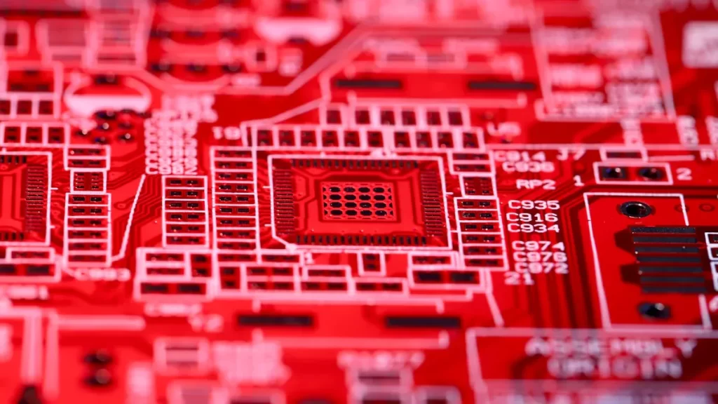
The SMT PCBA manufacturing process is essential for creating modern PCBs. It utilizes surface mount technology to attach components directly onto a circuit board, bypassing older methods and making the process faster and more efficient.
You might wonder why SMT PCBA manufacturing is so significant. Its precision ensures the production of high-quality boards. Proper solder paste printing is a critical factor, as poor application is responsible for most errors—up to 75% of issues stem from improper solder paste use. Additionally, SMT PCBA manufacturing is incredibly fast. A single machine line can place up to 100,000 components per hour, making it ideal for large-scale production.
By accelerating production and enhancing quality, SMT PCBA manufacturing has revolutionized the way electronics are built. Whether understanding its steps or its role in PCB assembly, SMT PCBA manufacturing ensures today’s devices are both reliable and efficient.
Key Takeaways
SMT PCBA manufacturing uses a method to attach parts directly to boards. This makes the process quicker and more effective.
Correct solder paste printing is very important. About 75% of mistakes happen from bad application. Regular checks help stop errors and make boards better.
Machines place parts quickly and accurately. However, people are needed for small or special parts.
Checking parts after placement ensures they are secure and in the right spot. This helps make more good boards on the first try.
Testing at the end makes sure the PCBA works properly. This keeps it safe and reliable for users.
Preparation in SMT PCBA Manufacturing
Document Creation and Design Validation
The first step in SMT manufacturing is making correct documents. The design must meet all rules and work as needed. For example, rules like FDA 21 CFR 820.30(g) and ISO 13485, Section 7.3.7, stress testing designs in real or fake conditions. This ensures the product works for users and its purpose.
To do this, use data like user feedback, clinical tests, and real-world testing. These steps prove the design is ready to be made. A detailed report is needed to show the process and follow industry rules.
Regulation | Description |
|---|---|
FDA 21 CFR 820.30(g) | Says device design must match user needs. |
ISO 13485, Section 7.3.7 | Requires testing to confirm the product works as intended. |
Solder Paste Printing
Solder paste printing is a key part of SMT manufacturing. It applies solder paste to the PCB using a stencil for placing parts. The quality of this step affects the product’s reliability. Important factors like paste volume, area, and height must be checked. For example, too little height causes weak joints, while too much can create solder bridges.
Metric | Importance | Impact on Reliability |
|---|---|---|
Volume | Ensures enough paste for good soldering | Prevents problems like cold joints |
Area | Covers all needed pads properly | Avoids connection issues |
Height | Needed for strong solder joints | Stops weak joints or solder bridging |
Regular checks of solder paste ensure these factors are correct. This step reduces mistakes and helps move smoothly to the next stage.
Stencil Inspection and Alignment
Before printing solder paste, check and align the stencil carefully. This ensures the paste goes on the PCB correctly. Problems like wrong layouts, missing parts, or misplaced fiducials can cause issues. For instance, even a small stencil misalignment can lead to assembly defects.
By checking for errors like wrong squeegee direction or missing fiducials, you can avoid costly problems. Correct alignment ensures the paste is placed exactly where needed, improving the process accuracy.
Tip: Always check stencils and align them well to avoid mistakes and keep quality high.
Component Placement in the SMT Manufacturing Process
Automated Component Placement
Placing parts automatically is a key step in SMT. Machines with advanced tools place parts on the PCB. They use fast systems to position resistors, capacitors, and ICs. This ensures accuracy and reduces mistakes made by people.
The benefits of automated placement include:
Ability to handle different part types.
Precise placement of small chips.
Shorter assembly times.
Easy handling of mixed part sizes.
Better planning for part placement.
Using machines for this step boosts speed and keeps quality high.
Manual Placement for Special Components
Even with automation, some parts need manual placement. These include odd-shaped parts, connectors, or fragile components. Skilled workers carefully place these parts to ensure they fit well.
Manual placement is needed for parts that need extra care. For example, large connectors or delicate pieces may not work with machines. By mixing manual and machine methods, you can meet special assembly needs.
Quality Checks After Placement
After placing parts, checks are done to ensure quality. These checks confirm all parts are in the right place and secure. Metrics like first-pass yield (FPY) show how many assemblies pass without fixes. A good FPY is 98-99%, showing high quality.
Other checks include tracking defects and testing reliability. These help find problems early, so the product meets customer needs. By keeping strict checks, you can make reliable PCB assemblies.
Tip: Check quality often to improve your SMT process and lower errors.
Soldering in SMT PCBA Manufacturing
Reflow Soldering Process
Reflow soldering is a common way to join parts in SMT. It heats the solder paste applied earlier to connect parts to the PCB. The process uses controlled heat to melt and solidify solder without harming parts.
Careful control during reflow soldering reduces problems like weak joints. Adjusting the heat profile strengthens solder joints and lowers electrical failure risks. The table below shows steps to improve soldering quality:
Impact on Defects | |
|---|---|
Precise Solder Paste Application | Stops issues like solder bridges, cold joints, or weak soldering. |
Optimized Component Placement | Prevents misaligned parts, tombstoning, or tilted components that cause failures. |
Controlled Reflow Soldering Process | Strengthens solder joints, reduces voids, and lowers defect risks. |
Thorough Inspection and Quality Control | Finds problems early, ensuring reliable and high-performing products. |
Tip: Always check the reflow oven’s temperature to keep soldering consistent.
Wave Soldering for Through-Hole Components
Wave soldering works well for through-hole parts in PCB assembly. It uses molten solder waves to solder many connections at once, making it fast and efficient.
Wave soldering is great for handling large amounts of through-hole parts quickly. It ensures even soldering, lowering the chance of mistakes. The table below compares wave soldering to other methods:
Advantage | Wave Soldering | Alternative Techniques |
|---|---|---|
Faster | Slower | |
Simultaneous Soldering | Yes | No |
Through-Hole Component Focus | Yes | Varies |
Wave soldering saves time and gives high-quality results in SMT PCBA manufacturing.
Common Soldering Defects and Their Prevention
Soldering mistakes can weaken PCB assemblies. Common problems include bridging, tombstoning, and poor wetting. Each issue has causes and fixes, as shown in the table below:
Defect Type | Description | Prevention Strategy |
|---|---|---|
Bridging | Solder connects pads, causing shorts. | Use pads that let extra solder flow away. |
De-wetting | Solder doesn’t stick well, often from bad paste. | Use clean surfaces and active solder paste. |
Tombstoning | Parts lift due to uneven soldering. | Heat all pads evenly to stop uneven cooling. |
Poor Wetting | Lead-free solder doesn’t stick to copper, causing weak joints. | Use finishes like ENIG to improve solder sticking. |
Component Shifting | Parts move during soldering. | Review designs and use proper placement methods. |
To avoid defects, train workers, standardize processes, and maintain equipment. These steps ensure better soldering and stronger PCB assemblies.
Testing in the SMT Manufacturing Process
Automated Optical Inspection (AOI)
Automated optical inspection checks the quality of PCB assembly. It uses cameras to find mistakes in soldering and part placement. AOI can spot tiny errors, which is important for crowded PCBs. It looks at solder joints and part values, making it useful for many tasks.
AOI is very flexible. It can be used at different steps, especially after soldering. Finding problems early saves money and time. Fixing mistakes during this step costs less than fixing them later.
Key Benefits of AOI:
Finds small placement errors.
Checks solder joints and part values.
Improves efficiency by catching mistakes early.
Can be used at many production stages.
X-Ray Inspection for Hidden Joints
X-ray inspection finds hidden problems in PCB assembly. It shows inside parts without breaking them. This helps check solder joints, part placement, and fake parts. X-rays can also find tiny cracks or hidden issues that might cause failures.
This method improves quality by reducing mistakes. It works well for checking solder joints under parts like BGAs. X-rays also help find the cause of problems during failure analysis.
Applications of X-Ray Inspection:
Verifies part placement.
Examines internal structures.
Detects fake parts.
Helps find causes of failures.
In-Circuit Testing (ICT) and Flying Probe Testing
In-circuit testing and flying probe testing check if PCBs work. ICT uses a fixed “bed-of-nails” to test connections. It is fast and good for making many boards. Flying probe testing uses moving probes, making it better for small batches or new designs.
Each method has its strengths. ICT is faster and covers more, while flying probe testing is cheaper and more flexible. Using both methods ensures thorough testing for all needs.
Aspect | In-Circuit Testing (ICT) | Flying Probe Testing |
|---|---|---|
Fixture | Fixed “bed-of-nails” | Movable probes |
Speed | Faster for large production | Slower but flexible |
Cost | Higher for small runs | Lower for small batches |
Flexibility | Less flexible for changes | Very flexible |
Coverage | Tests many things | High test coverage |
These tests make sure PCBs are high-quality and work properly.
Functional Testing for Final Validation
Functional testing is the last step to check if your PCBA works properly. It tests how the board performs in real-life situations. This ensures all parts work together and meet the design’s needs.
In this step, you recreate the environment where the PCBA will be used. For instance, if it’s for a medical device, you test it in similar conditions. This makes sure the product is safe and reliable.
Key Steps in Functional Testing:
Test Setup: Connect the PCBA to tools that mimic its real use.
Input Simulation: Send signals, power, or data to the board.
Output Verification: Check if the outputs match what’s expected.
Stress Testing: Test the board in tough conditions like heat or high voltage.
Tip: Always write down test results. This helps track issues and improve performance.
Functional testing has many advantages:
It ensures the PCBA meets customer needs.
It lowers the chance of failures after delivery.
It helps follow industry rules and standards.
Test Type | Purpose | Example |
|---|---|---|
Input Simulation | Tests how the board handles inputs | Adding voltage to power pins |
Output Verification | Confirms correct output signals | Checking signal strength |
Stress Testing | Checks reliability under stress | Testing in high heat |
By doing functional testing, you can deliver a reliable product. This step builds customer trust and ensures long-term success.
Final Steps in SMT PCBA Manufacturing
Cleaning the PCB and Removing Debris
Cleaning the PCB is very important for its reliability. During assembly, dirt, flux, and other residues can build up. These can cause corrosion, electrical leaks, or short circuits if not cleaned. Methods like ultrasonic, solvent, or water-based cleaning can remove these effectively.
Studies show cleaning improves PCB quality. For example:
Study | Findings |
|---|---|
Belton et al. (2008) | Removing sources greatly lowers PCB contamination. |
Majcher et al. (2022) | |
Payne et al. (2019) | Advanced cleaning reduced PCB levels by 52%. |
Using proper cleaning methods makes PCBs last longer and work better.
Adding a Protective Coating
A conformal coating protects the PCB from moisture, dust, and chemicals. This step helps the board last longer, especially in tough conditions. Cleaning the PCB first ensures no dirt gets trapped under the coating.
Benefits of conformal coating include:
Stops corrosion by increasing insulation resistance.
Prevents leaks caused by leftover flux.
Gives strong protection when applied to clean boards.
Always clean the PCB well before coating it. This helps the coating stick better and protect more.
Final Checks and Packaging
The last step is checking the PCB assembly to meet standards. This includes visual checks, size measurements, and testing how it works. You also check materials and packaging for safe delivery.
Important steps include:
Looking for visible defects.
Testing to ensure the board works properly.
Checking packaging for safe transport.
Random checks before shipping are also important. Sampling batches can find problems and fix them early. These checks ensure the PCB assembly is ready and reliable for use.
The SMT process has many important steps, like preparation and testing. Steps such as solder paste printing, placing parts, and testing are crucial. Each step ensures the PCBAs are reliable and work well. Following these steps reduces mistakes and creates better boards.
SMT PCBA manufacturing changed how electronics are made. It helps build small, efficient, and dependable devices for today’s needs. Learning about this process shows the care and creativity in modern technology.
FAQ
What does SMT mean in PCBA manufacturing?
SMT means Surface Mount Technology. It places parts directly on a PCB. This method is faster and works well for small designs.
Why is solder paste printing important?
Solder paste printing connects parts to the PCB correctly. If done wrong, it can cause weak joints or shorts. Using the right amount improves product reliability and performance.
Tip: Check solder paste for volume, area, and height to avoid problems.
How does automated optical inspection (AOI) work?
AOI uses cameras to find mistakes in soldering or part placement. It spots problems early, saving time and money. This ensures the PCB meets quality standards before the next step.
Can SMT handle every type of component?
No, SMT is best for small parts. Bigger or odd-shaped parts, like connectors, need manual placement. Using both methods ensures all parts fit well.
What is functional testing for?
Functional testing checks if the PCB works in real-life situations. It ensures safety, reliability, and good performance. This step makes sure the product meets customer needs and rules.
Emoji Reminder: 🛠️ Testing ensures your electronics are dependable!
See Also
An In-Depth Overview of Steps in PCBA Production
Enhancing Workflow Productivity in PCBA Manufacturing Processes
Investigating Testing Methods for Advanced PCBA Electronics
Significance of PCBA Test Jigs in Today’s Electronics Manufacturing