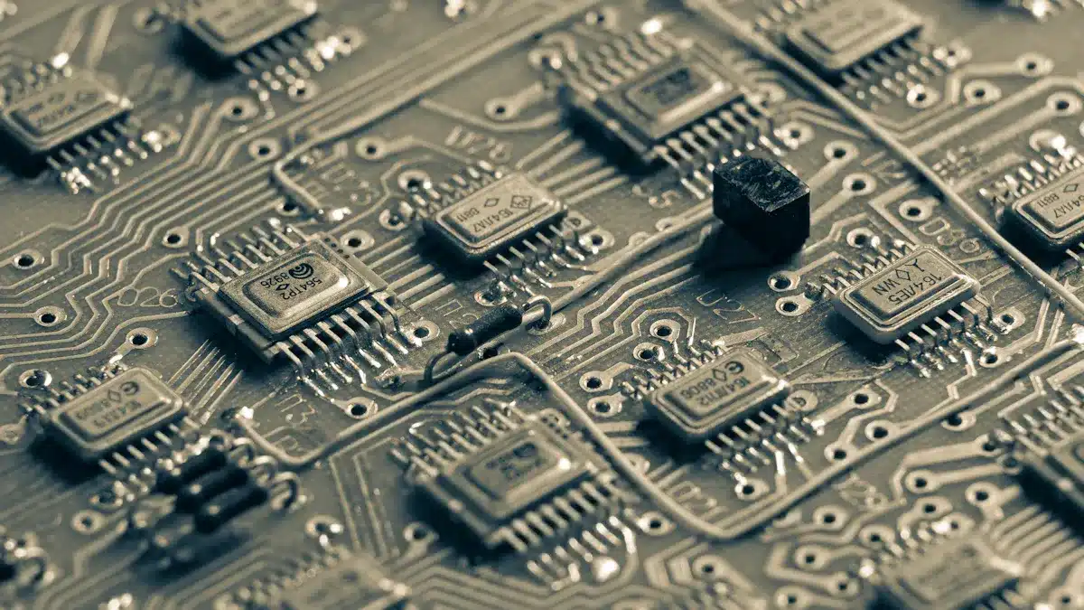
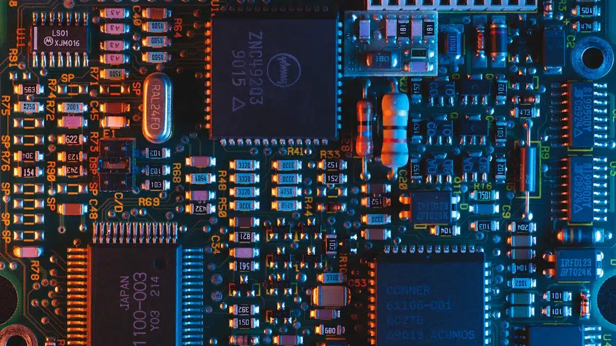
You enter the world of electronics when you start assembling circuit boards and learn about the PCB assembly process. Every printed circuit board begins as a blank board. You go through steps like solder paste application, component placement, and inspection. These careful steps prevent mistakes and help products last longer.
Quality control uses visual checks, automated optical inspection, and testing. These methods help you find problems early and keep every printed circuit board working well. When you understand each step of assembling circuit boards, you make circuit board assembly faster and more reliable. This applies to both surface mount and through-hole technology.
Key Takeaways
Begin PCB assembly with good planning and design. This helps stop problems and makes work faster.
Put solder paste on carefully with the right tools. Check your work to stop mistakes and make strong joints.
Use machines to place parts. This makes things fast, correct, and the same each time.
Pick the best soldering way for each job. Use reflow for small parts. Use wave for through-hole parts. Use hand soldering to fix things. This helps make strong connections.
Check and test boards well. Look at them, use AOI, X-rays, and do tests. This helps find problems early and keeps quality high.
PCB Assembly Process Steps
The pcb assembly process turns a blank printed circuit board into a working device. Each step builds on the last one. This helps you get a reliable and high-quality product. You start with design and preparation. Then you apply solder paste and place components. These steps connect and prepare for soldering, inspection, and testing.
Design for Assembly
You start with design for assembly. This step shapes the whole printed circuit board assembly process. Good design and planning help you avoid problems later. You check the layout and make sure all electrical connections are right. You also confirm the board meets mechanical and thermal needs. You review the Bill of Materials (BoM) and gather all the parts before you begin.
Tip: If design, fabrication, and assembly teams work together early, they can find and fix problems before they become expensive.
Design for assembly (DFA) makes the printed circuit board easier to build. You place components in smart spots and balance copper on the board. You also pick strong materials. These actions help stop defects like solder bridging, tombstoning, and warpage. DFA also suggests using standard parts and simple layouts. This makes production faster and lowers costs.
Lower assembly defects and rework.
Make solder joints better.
Get products to market faster.
Raise first-pass yield.
When you plan for manufacturability, the pcb assembly process goes smoother and faster.
Solder Paste
Next, you apply solder paste. This step gets the printed circuit board ready for placing components. You use a stencil to put solder paste only where it is needed. The quality of this step affects almost every part of the printed circuit board assembly.
Solder paste comes in different types. You can pick leaded or lead-free pastes. Leaded solder paste melts at lower temperatures. Lead-free pastes meet environmental rules and use metals like tin, silver, and copper. You also choose the right particle size and flux type for your job.
Types / Examples | Description | |
|---|---|---|
Particle Size | Type 1 to Type 8 | Smaller particles allow for finer, more precise printing. |
Flux Type | Rosin, Water-soluble, No-clean | Each type affects cleaning needs and residue. |
Material Composition | Leaded, Lead-free | Lead-free pastes are RoHS compliant and better for the environment. |
How you apply solder paste is important. Up to 75% of SMT defects come from bad solder paste printing. You need the right stencil, blade angle, and printing speed. Solder Paste Inspection (SPI) helps you find problems early, like too much or too little paste. This early check saves time and cuts down on waste.
Key things for good solder paste application:
Use a smooth, burr-free stencil.
Set blade speed and pressure right.
Support the PCB to keep paste even.
Clean the stencil often.
If you control these things, you get strong solder joints and fewer defects in your printed circuit board.
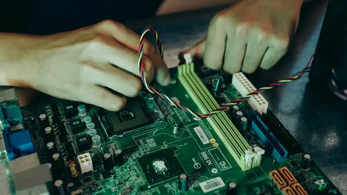
Placement
After solder paste, you place components on the printed circuit board. This step uses both Surface Mount Technology (SMT) and Through-Hole Technology (THT), depending on your design.
For SMT, you use automated pick-and-place machines. These machines work fast and are very accurate. They use cameras to line up each part just right. You load parts into feeders. The machine picks them up and puts them on the board. Automated placement can be very precise, down to ±0.03 mm. This accuracy lowers mistakes and keeps quality high.
Feature | Manual Placement | |
|---|---|---|
Speed | Slow, labor-intensive | Fast, ideal for large batches |
Placement Accuracy | Limited by human skill | High precision, minimal errors |
Consistency and Repeatability | Hard to maintain | Consistent, reliable results |
Damage Risk | Higher | Lower, gentle robotic handling |
Scalability | Not efficient | Scalable for mass production |
Manual placement is still used for small jobs or tricky boards. But automated systems give you speed, accuracy, and repeatability that manual work cannot.
After placement, you check the board. Automated Optical Inspection (AOI) looks for missing or wrong parts. You can also use electrical tests to make sure everything works.
Remember: Careful placement helps make strong solder joints and a reliable printed circuit board assembly.
Soldering Methods
Soldering connects electronic parts to your printed circuit board. You pick a method based on your board and how many you need. Each way has its own use and good points.
Reflow Soldering
Reflow soldering is the main way for SMT components. First, you put solder paste on the pads. Then, you place the parts on the paste. The board goes into a reflow oven. The oven heats the board in steps to melt the solder. This makes strong joints. You must watch the heat and cooling. This keeps parts safe and joints strong.
Preheat the board
Hold at a steady temperature
Melt the solder (reflow)
Cool down slowly
Reflow soldering is best for crowded boards and big batches. You can use it for one or both sides of a board. You need to check the heat to protect weak parts.
Tip: Always check the solder paste and board before setting oven heat.
Wave Soldering
Wave soldering works best for through-hole components. You put parts into holes on the board. The board moves over a wave of hot solder. The solder joins the leads to the pads. This way is fast and good for making many boards.
Good things about wave soldering:
Great for making lots of boards
Makes strong joints
Saves money for through-hole parts
Not for tiny SMT parts
High heat can hurt weak parts
Can cause solder bridges and bent boards
Wave soldering is good for mixed boards but is used less now because SMT is more common.
Hand Soldering
Hand soldering uses a soldering iron and wire solder. You use this for test boards, fixing, and small jobs. It lets you work on special parts and make changes. You also use it to fix things after machines finish.
When to use hand soldering:
Small jobs
Test boards and fixing
Special or custom parts
Fixing after machine soldering
Hand soldering is flexible but slow and needs skill. You cannot use it for very tiny parts like BGAs.
Typical Use | Advantages | Limitations | |
|---|---|---|---|
Reflow Soldering | SMT components | High precision, automated | Needs careful temperature control |
Wave Soldering | Through-hole components | Fast, strong joints | Not for fine-pitch SMT |
Hand Soldering | Prototypes, repairs, custom | Flexible, adaptable | Slow, labor-intensive |
Picking the right soldering method helps you make strong and good circuit boards.
Inspection and Testing
Inspection and testing help you spot problems early. These steps make sure your circuit boards work well. You use different ways to check for defects. You also make sure each board meets quality rules. These steps are important because they stop bad products from reaching customers.
Visual and AOI
First, you do a visual inspection. You look for easy-to-see problems. These include parts that are not lined up, broken traces, or bad solder joints. Manual inspection is good for small batches. But people can miss hidden problems. Automated Optical Inspection (AOI) uses cameras and special software. AOI scans the board fast and finds missing parts, solder bridges, open circuits, and placement mistakes. AOI is much faster and more accurate than checking by hand.
AOI helps you find problems like:
Solder bridges that cause shorts
Too much or too little solder
Lifted leads and parts in the wrong place
Defects Detected | Advantages | |
|---|---|---|
Visual | Solder joints, placement, damage | Low cost, easy to use |
AOI | Soldering, missing/misaligned parts | Fast, precise, repeatable |
AOI is very important in modern PCB assembly. You use it to check boards quickly and keep quality high.
X-ray Inspection
Some problems hide under parts or inside the board. You use X-ray inspection to see these hidden issues. X-rays go through the board and show solder voids, bridges, cold joints, and cracks. This way does not hurt the board. X-ray inspection is needed for tricky boards with BGAs or QFNs.
X-ray inspection finds:
Solder voids that make joints weak
Hidden solder bridges that cause shorts
Cracks inside the board
You use X-ray inspection for products that must work very well, like medical devices and aerospace electronics.
Functional Testing
After inspection, you test the board to make sure it works. Functional testing gives power to the board and checks how it acts. You measure voltage, check signals, and test ports. You use tools like multimeters, oscilloscopes, and signal generators. You also do load tests and stress tests to see how the board handles heat, shaking, and wetness.
Functional testing helps you:
Find short circuits and open circuits
Make sure parts are in the right place
Check that the board works as planned
You make a test plan, run the tests, and fix any problems before shipping. These steps make sure your PCB is strong and ready to use.
Through-Hole and Hybrid Assembly
Through-Hole Assembly
You use through-hole technology when you want strong connections. This method is good for projects that need to last a long time, like military or aerospace electronics. In through-hole technology, you put component leads into drilled holes. Then you solder them on the other side of the board. This makes a strong bond that can handle stress.
Here are the main steps for through-hole technology:
Design and drill the PCB with holes for each lead.
Put the components into the holes and line them up.
Solder the leads by wave soldering, selective soldering, or by hand.
Check the solder joints and test the electrical connections.
Cut off extra leads to keep the board neat and safe.
You often pick through-hole technology for testing or hobby projects. It is easier to fix and test by hand. The solder goes through the hole and connects both sides of the board. This gives you a strong joint. You can use wave soldering for big batches or hand soldering for small jobs.
Through-Hole Technology | Surface Mount Technology (SMT) | |
|---|---|---|
Component Mounting | Leads go in holes and are soldered on the other side | Leads are soldered right to the surface; no holes needed |
Assembly Method | Manual or wave soldering; easier to solder by hand | Automated pick-and-place and reflow soldering |
Mechanical Strength | Stronger bond; good for high-reliability | Less strength; good for small, compact designs |
Tip: Use through-hole technology when you need strong support or want to make changes while testing.
Hybrid Assembly
Hybrid assembly lets you use both methods together. You use surface mount technology for small, light parts. You use through-hole technology for big or heavy parts. First, you place and solder surface mount parts with machines. Next, you add parts that need more strength with through-hole technology.
Use surface mount technology for tight spaces and fast work.
Save through-hole technology for connectors, big capacitors, or parts that get pulled or pushed.
Hybrid assembly helps you make boards that are small but also strong.
You often see hybrid assembly in cars, factories, or military electronics. This way gives you more choices and makes sure your board is both small and tough.
Note: Hybrid assembly lets you design boards that hold both delicate and strong parts.
Cleaning and Final Steps
Cleaning
You need to clean your printed circuit board after it is made. Cleaning gets rid of flux, dust, and other dirt. If you do not clean, the board can rust or work badly. There are different ways to clean:
Manual cleaning uses soft brushes and wipes with special cleaners. Isopropyl alcohol (IPA) helps remove sticky flux. Some cleaners work better for tough spots.
Water-based cleaning uses pure water and soap for water-soluble flux. You must rinse well so the board does not rust.
Ultrasonic cleaning uses sound waves in liquid. This method cleans small spaces and is good for crowded boards.
Automated cleaning uses machines that spray or dip boards. These are best for making many boards and give the same results each time.
Dry cleaning uses air, special brushes, or safe vacuums. These remove dust without using any liquid.
Tip: Pick a cleaning way that matches your flux type. Always dry your board fully after cleaning so it does not get wet inside.
Final Inspection
You must check your board before you pack it. Final inspection looks for mistakes and checks if the board is strong. Trained inspectors use different ways:
Visual inspection finds problems you can see, like bad solder, missing parts, or cracks.
Automated Optical Inspection (AOI) uses cameras to compare your board to a good one. AOI finds mistakes fast and tells you how bad they are.
X-ray inspection looks inside the board for hidden problems, like bad solder or broken parts.
In-Circuit Testing (ICT) checks if the board works, if parts are right, and if all paths connect.
Functional testing acts like real use. You turn on the board and check signals, ports, and programs.
These checks follow rules like UL, ISO, IPC, and RoHS. Only good boards go to the last steps and get packed.
Packaging
You must keep your boards safe when you ship or store them. Good packaging stops water, bumps, and static from hurting the boards. You can use many ways:
Moisture barrier bags and drying packs keep water away from the board.
Vacuum sealing takes out air and water from the package.
Strong boxes and foam keep boards from moving and breaking.
Humidity cards let you check if the board gets wet.
Do not put too many boards in one box. Use stiff boards to protect thin ones.
Put labels on each package with part numbers, dates, and how many are inside.
Note: Keep your boards in their first package so they stay safe and dry.
You end by packing, writing down details, and checking quality. These steps help your boards arrive safe and ready to use.
Assembling Circuit Boards: Key Stages
SMT vs. THT
When you build circuit boards, you pick SMT or THT. Each way has its own steps and good points. SMT is used in most new electronics. It is great for making lots of boards fast. THT is still used when you need strong connections or special parts.
Here are the main steps for SMT:
Put solder paste on the PCB pads with a stencil.
Check the solder paste for problems and fix them.
Place surface mount parts on the paste using machines.
Heat the board in a reflow oven to melt the solder.
For THT, you follow these steps:
Drill holes in the PCB for each part lead.
Put the leads through the holes in the right spot.
Check and fix the placement if needed.
Solder the leads, often with wave soldering.
SMT does not need holes for leads. This makes building boards faster and cheaper for big batches. THT takes more time and work but gives stronger bonds.
Aspect | Surface Mount Technology (SMT) | Through-Hole Technology (THT) |
|---|---|---|
Slower, more manual | ||
Cost | Lower for large runs | Higher for mass production |
Setup Investment | High machinery cost | Lower setup cost |
Use Case | Best for high-volume | Good for small batches |
Mixed Technology
Sometimes you use both SMT and THT on one board. Mixed technology lets you use the best parts of each way. You get more choices and stronger boards. You can put small parts with SMT. You use THT for big or hot parts.
You can use SMT, THT, and BGA parts together.
Through-hole parts make strong bonds.
You can place parts where they work best.
You can use parts only made for through-hole.
It helps with heat for parts that get hot.
You get more choices and better performance.
Production is faster with smart machines.
Challenges of mixed technology:
Making the board is harder with more steps.
It costs more because you need extra work.
It is tricky to balance SMT and THT parts.
Boards can be bigger because through-hole parts need space.
Soldering can be tough, especially keeping SMT parts safe.
It is harder to change through-hole parts than SMT.
You see mixed technology in cars, medical tools, and factory controls. Using both ways makes boards strong and flexible. You need to plan well to get the best results.
Tip: Mixed technology helps you make boards that are small, tough, and ready for hard jobs. You get the good parts of both ways when you build with mixed technology.
You now know the main steps in PCB assembly. These steps include design, soldering, inspection, and testing. Each step is important for making good boards. Doing each step carefully helps you stop mistakes and make strong boards.
The most important things for good PCBs are:
Picking the right parts
Smart PCB design
Good soldering
Careful testing
Clean workspace
If you want to learn more or need help, many companies can help you. They offer special services and learning tools:
Description | |
|---|---|
Custom Solutions | PCB assemblies made just for you |
Advanced Testing & QC | Careful tests for strong and lasting boards |
Assembly Technologies | SMT, THT, BGA, fine pitch, and more |
Educational Resources | PCB schools and guides to help you learn |
Remember, every circuit board takes skill and care to make!
FAQ
What is the difference between SMT and THT?
SMT stands for Surface Mount Technology. You place parts on the surface of the board. THT means Through-Hole Technology. You put part leads through holes in the board. SMT works best for small parts. THT gives stronger connections.
Why do you need to clean a PCB after assembly?
Cleaning removes flux, dust, and dirt. If you skip cleaning, your board may not work well. Dirt can cause short circuits or corrosion. Clean boards last longer and perform better.
How do you check for defects in a PCB?
You use visual checks, AOI machines, and X-ray inspection. AOI uses cameras to spot missing or wrong parts. X-ray finds hidden problems. You also test the board to make sure it works.
Can you mix SMT and THT on one board?
Yes, you can use both methods. SMT works for small parts. THT is good for big or strong parts. Mixing them helps you build boards that are small and tough.
What happens if you use too much solder paste?
Too much solder paste can cause solder bridges. These bridges create short circuits. You may also see weak joints or parts that move. Always check the amount of paste before soldering.
See Also
Key Stages Involved In The PCBA Production Process
A Clear Overview Of PCBA Assembly And Manufacturing
Exploring The SMT Process Within PCBA Assembly Workflow