You can have many problems when working with printed circuit assembly. Soldering mistakes, design problems, and trouble finding parts can make pcba results bad. This step-by-step guide helps you get through these problems. It also helps you feel sure about each part of the process. Here are some common problems and ways to fix them:
Challenge | Solution |
|---|---|
Use good solder and reflow ovens for stronger joints. | |
Use pick-and-place machines and check quality often. | |
Thermal management | Use heat sinks and thermal checks to keep parts safe. |
Component sourcing | Buy from trusted suppliers and look out for fake parts. |
You can stop expensive mistakes in pcb assembly. Just follow best steps and check quality at every pcba stage.
Key Takeaways
Follow clear steps from design to final assembly. This helps you avoid mistakes. It also helps you build good circuit boards.
Use trusted suppliers for your parts. Check all parts carefully before you start assembly. This stops delays and defects.
Clean your boards well before and after assembly. This helps make strong solder joints. It also helps your boards last longer.
Check your boards at every stage. Use your eyes, machines, and tests to find problems early.
Protect finished boards with good packaging. Add all needed papers. This keeps boards safe and easy to use.
Printed Circuit Assembly Overview
What Is PCBA?
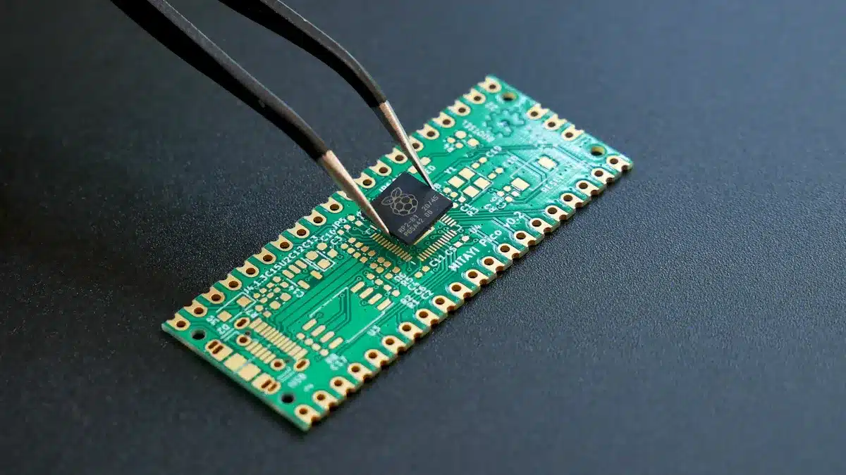
You might ask how a printed circuit board starts working. The answer is pcb assembly, or pcba. In this step, you take a bare pcb and put electronic parts on it. A printed circuit board without assembly is just a flat board with copper lines and holes. When you add resistors, capacitors, chips, and connectors, the board can do its job.
Here is how printed circuit assembly fits into the whole process:
PCB manufacturing makes the bare pcb by etching copper, drilling holes, and adding layers.
PCB assembly, or pcba, puts electronic parts on the board using special machines and tools.
The finished pcba gets tested to make sure it works right.
Note: PCB manufacturing and pcb assembly are not the same. Manufacturing gives you the empty board. Assembly adds the parts to make it work.
You can see the main differences in this table:
Aspect | PCB Manufacturing (Fabrication) | PCB Assembly (PCBA) |
|---|---|---|
Definition | Making the bare board with copper lines and holes | Putting electronic parts on the bare board |
Function | Gives support and paths for electricity | Makes a working electronic circuit |
Components | No parts (just the board) | Has resistors, capacitors, ICs, connectors, and more |
Process Steps | Etching copper, adding solder mask, drilling holes | Solder paste, placing parts, soldering |
Techniques | Uses etching and drilling | SMT, Through-Hole Technology, reflow and wave soldering |
Testing | Checks copper lines for breaks or shorts | Tests if the board works and looks right |
Outcome | Bare PCB ready for assembly | Finished, working PCB (PCBA) |
Key Techniques: SMT and THT
There are two main ways to do printed circuit assembly: Surface Mount Technology (SMT) and Through-Hole Technology (THT). Each way has its own good points.
SMT puts surface mount parts right onto the pcb surface. Machines do this fast and very accurately. SMT lets you put more parts on both sides of the pcb. This way is best for small, light parts and making lots of boards.
THT puts parts with leads through holes in the pcb. You then solder these leads on the other side. THT makes stronger bonds. You use THT for parts that need to handle stress or heat.
Aspect | Surface Mount Technology (SMT) | Through-Hole Technology (THT) |
|---|---|---|
Assembly Method | Parts soldered right onto the pcb surface; done by machines | Parts put into holes; soldered by hand or with wave soldering |
Mechanical Strength | Weaker bonds; depends on solder joints | Stronger bonds; leads go through the pcb for strength |
Manufacturing Efficiency | Faster and more efficient; uses machines | Slower; takes longer; needs more hand work |
Component Size & Density | Smaller parts; more parts fit; both sides of pcb used | Bigger parts; fewer parts fit; holes limit where parts go |
Cost | Cheaper because no drilling and uses machines | Costs more because of drilling and hand work |
Environmental Resistance | Not as strong against heat or stress | Handles heat and stress better |
Typical Use Cases | Used for making many boards, small devices, and tight spaces | Used for testing, strong parts, and aerospace |
Most of the time, both SMT and THT are used in one pcba. This gives you the good parts of each way. When you know about these methods, you can pick the best way to build your printed circuit assembly.
Design for Assembly (DFA)
Design for Assembly (DFA) helps your pcb and pcba projects work well. If you use DFA rules, you can stop mistakes early. This makes the assembly process faster and easier. You also save time and money when you build and test your boards.
Design Files
You must get all your design files ready before assembly. These files help with every step, from first build to finished pcba. Here is what you need to include:
Gerber files for copper layers, solder mask, silkscreen, and paste layers.
Drill files in Excellon format with tool codes and hole sizes.
Board outline that shows any cutouts or slots.
Fabrication drawings with board thickness, copper weight, and special needs.
Bill of Materials (BOM) for all parts you need.
ReadMe or other files for extra notes or help.
Tip: Always check your files before you send them out. If files are missing or wrong, your project can be delayed.
BOM Review
A clear BOM (Bill of Materials) helps make assembly go smoothly. Your BOM should list every part needed for your pcb, like:
Descriptions to tell parts apart
How many of each part you need
Unit of measure (each, foot, etc.)
How you get the part (buy, make, or change)
Reference designators for where parts go on the pcb
Notes for special steps or other suppliers
Make your BOM early when you start building your board. This helps you plan, save money, and not miss any parts. Check and update your BOM often as your design changes.
Note: Ask your manufacturing partner for help early. They can find problems in your design or BOM before you start assembly.
If you follow DFA rules, like putting related parts close together and using common parts, your pcb is easier to build. Clear labels and working with your assembly partner early help stop mistakes and make building and testing faster.
Component Procurement
Sourcing
You must find the right electronic parts before building your pcb. Getting parts from good sources helps you avoid delays and problems. A strong vendor network with trusted distributors gives you real parts, even when there are shortages. Distributors like DigiKey, Mouser, and Arrow Electronics work with companies like Texas Instruments and Murata. These partnerships help you get parts that are real and can be tracked.
When picking suppliers, always check their background. Look for certifications like ISO 9001 or AS9120. Ask for certificates or test reports to make sure the parts are right. You can lower risks by using more than one supplier and checking your inventory often. This helps you avoid running out of parts, getting fake parts, or using old parts. The electronics industry loses a lot of money each year to fake parts, so you must be careful.
Here are some good ways to find parts:
Use special buying systems to manage orders and track deliveries.
Check vendors by looking at things like on-time delivery and order accuracy.
Follow rules like RoHS and REACH to stay out of legal trouble.
Save money by comparing prices and talking with suppliers.
Use just-in-time delivery and plan ahead to keep less inventory.
Tip: Always keep records of your suppliers and parts. Good records help you track and check quality.
Incoming Quality Control
After you get your parts, you must check them before starting pcb assembly. Checking parts first makes sure they meet your standards. Start by checking the part name, amount, batch number, maker, and date. This step helps you track each part during the pcba process.
You should also check the Bills of Materials to make sure you got the right parts. Use sampling plans like AQL to decide how many to check. Third-party inspectors can help by sending samples to labs for testing.
Common ways to check quality include:
Visual inspection: Look for cracks, scratches, or other problems.
Dimensional inspection: Measure size and shape to match what you need.
Physical performance tests: Test things like hardness and strength.
Chemical analysis: Check what the part is made of for hidden problems.
Non-destructive inspection: Use X-ray or sound to find inside problems.
Electrical and thermal tests: Make sure the parts work as they should.
You should also check your suppliers’ quality systems. This makes sure they follow the right steps and record any problems. Careful checks now help you avoid problems later and make your pcba better.
PCB Preparation
Cleaning
You need to start with a clean pcb before you add any parts. Dust, oil, and leftover chemicals can cause problems during assembly. Cleaning helps you avoid soldering defects and keeps your board reliable.
Here are some common cleaning methods:
Ultrasonic Cleaning: Place the pcb in a bath with deionized water. Ultrasonic waves shake off dirt and flux. After cleaning, rinse with deionized water and dry the board.
Aqueous and Semi-Aqueous Cleaning: Wash the pcb with water-based or mixed solutions. Rinse well and dry to remove any leftover chemicals.
Vapor Degreasing: Expose the pcb to hot solvent vapors. The vapors dissolve oils and grease. Rinse and dry the board after this step.
Solvent-Based Cleaning: Use isopropyl alcohol (IPA) with a brush or wipe. IPA removes flux and oils quickly and leaves no residue.
Dry Cleaning: Blow off dust with compressed air or use a soft brush for stubborn particles.
Tip: Always use deionized water for rinsing. This prevents corrosion and keeps your pcb safe.
Choose the cleaning method based on the type of dirt or residue. Make sure you dry and inspect the board after cleaning. This step helps you catch any leftover contaminants before moving on.
Stencil Making
Stencils help you put solder paste exactly where you need it on the pcb. A good stencil makes sure each pad gets the right amount of paste, which helps you avoid soldering problems.
You can use different materials for stencils, such as stainless steel, copper, or nickel. Stainless steel is the most common because it is strong and lasts a long time. For fine-pitch parts, nickel works best.
Stencil thickness usually ranges from 0.1 to 0.2 mm. Thinner stencils work for small parts, while thicker ones suit larger pads.
Apertures, or holes in the stencil, are often 10-20% smaller than the pads on the pcb. This helps prevent too much solder paste and stops bridging.
Multilevel stencils can have different thicknesses for different parts.
You should clean the stencil after every 5-10 uses to keep the apertures clear.
Store stencils flat in a dry, dust-free place to avoid bending or damage.
Note: Use fiducial marks on both the pcb and stencil to help with alignment. This ensures the solder paste goes exactly where you want it.
Solder Paste Application
Stenciling
You begin by putting a stencil on your pcb. The stencil is a thin metal sheet with small holes. These holes match the spots where parts will go. You use a squeegee to spread solder paste over the stencil. The paste goes through the holes and lands on the right pads.
To do this well, follow these steps:
Make sure your workspace is clean and bright. Hold your pcb in place.
If the solder paste was cold, let it warm up first.
Put the stencil on the pcb and line up the marks.
Spread the solder paste across the stencil with a squeegee.
Lift the stencil slowly so you do not smear the paste.
Tip: Use just enough solder paste. Too much can cause shorts. Too little can make weak joints.
You can do stenciling by hand or with a machine. Machines are faster and more exact. They help when you need to make many boards. Clean your tools after using them. This keeps the solder paste fresh and stops dirt from getting in.
Paste Inspection
After you put on the solder paste, you need to check it. Checking helps you find problems early. This keeps your pcba process running well. There are a few ways to check the paste:
Manual inspection means looking at the pcb with your eyes or a magnifier. This is good for small jobs but may miss tiny mistakes.
Automated Optical Inspection (AOI) uses cameras and computers to look at the pcb. AOI can find missing or extra paste and uneven spots.
3D Solder Paste Inspection (SPI) checks the height, amount, and area of the paste. This way is the most exact. It helps you see if there is too much or too little paste.
Inspection Method | Description | Advantages | Disadvantages |
|---|---|---|---|
Manual | A person looks at the board | Good for special boards, flexible | Slow, can miss small mistakes |
AOI | Cameras take and compare pictures | Fast, finds many problems, accurate | Needs setup and care |
3D SPI | Checks paste size and shape | Most exact, finds hard problems | Costs more, needs special tools |
Note: Careful checking now helps you avoid fixing mistakes later in the pcba process.
Always check the solder paste before you add parts. This step makes sure your pcb will have strong and safe connections.
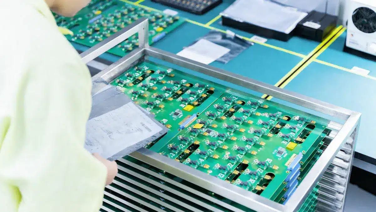
SMT Component Placement
Pick and Place
Pick and place machines put surface mount components on your PCB. These machines use a vacuum nozzle to pick up each part. They set the part down on the right pad. You load reels or trays of parts into the machine. The machine reads placement data from your assembly files. It works fast and can place hundreds of parts each minute. Pick and place machines handle many types of parts. They can work with tiny resistors and large chips. These machines are gentle with small and delicate parts. Most modern machines have cameras to check each part’s position. The camera checks before the part is placed. This helps stop mistakes and keeps the process smooth.
Tip: Keep your pick and place machine clean and in good shape. This helps stop jams and wrong placements.
Placement Accuracy
Accurate placement is very important in SMT assembly. If a part is not placed right, you can get soldering problems. You might also get short circuits. You want every part to sit right on the pads. Many things affect how accurate the placement is. Machine type, platform material, and temperature changes all matter.
Here is a table that shows how different machine platforms affect accuracy:
Machine Construction Material | Accuracy Limit (3σ) | Environmental Impact |
|---|---|---|
Aluminum-based platforms | 50 to 100 microns | Less stable, lower accuracy |
Steel-based platforms | ~20 microns | More stable, better accuracy |
Granite/Ceramic-based platforms | More accurate than aluminum/steel | Highest accuracy platforms |
Temperature variations | Can cause 20-30 microns shift | Even 5°F ambient change affects placement |
Steel and granite platforms give better accuracy than aluminum. Temperature changes in your shop can move parts out of place.
Most SMT assembly lines try for ±0.025 mm (25 microns) accuracy. High-precision machines can reach within 0.01 mm. You need to check and adjust your machines often. This helps keep them accurate. Automated Optical Inspection (AOI) checks if parts are within ±0.05 mm and within 1° of rotation.
Accuracy Aspect | Typical Accuracy Range | Notes on Calibration and Inspection |
|---|---|---|
General SMT Assembly | ±0.025 mm (25 microns) | Achieved through regular calibration |
High-precision calibration | Within 0.01 mm | Uses test boards with known reference points |
Automated Optical Inspection (AOI) | ±0.05 mm position, ±1° rotation | Ensures components are within acceptable tolerances |
You should always check your machines and boards for accuracy. Good placement means fewer problems and better working boards.
Reflow Soldering
Reflow soldering is a key step in making strong and reliable connections on your PCB. You use this process to melt the solder paste and attach surface mount parts to the board. The reflow oven heats the board in several zones, each with a special job.
Heating Process
You start with the heating process, which has four main zones. Each zone helps you get the best soldering results:
Preheat Zone: This zone slowly raises the temperature of your PCB. You want to avoid thermal shock and activate the flux in the solder paste. The temperature usually goes from 25°C to 150°C for leaded solder, or up to 180°C for lead-free. This step takes about 60 to 90 seconds. The temperature should rise at a rate of 1.5°C to 3°C per second.
Soak Zone: Here, you keep the board at a steady temperature. This helps the flux work and removes oxides from the pads and leads. The temperature stays between 150°C and 200°C for leaded solder, or 180°C to 220°C for lead-free. This zone lasts 60 to 120 seconds.
Reflow Zone: In this zone, the temperature rises above the melting point of the solder. The solder paste melts and forms strong joints. The peak temperature is 210°C to 240°C for leaded solder, or 240°C to 260°C for lead-free. You want the board to stay above the melting point for 30 to 60 seconds, but not too long. This prevents damage to the parts.
Tip: Always control the temperature profile. Uniform heating helps you avoid defects and makes the soldering process more reliable.
You can use different ovens for this process. Convection ovens give you even heating and better control. Infrared ovens heat up fast but may cause uneven results. Make sure you calibrate and maintain your oven for the best soldering quality.
Cooling
After the solder melts, you need to cool the board in a controlled way. The cooling zone lets the solder joints solidify. If you cool too fast, you can get cracks or weak joints. If you cool too slowly, the solder may form large grains and lose strength.
Use a cooling rate of about 3°C to 5°C per second.
Make sure the air flow is even across the board.
Check the joints after cooling for smooth, shiny surfaces.
A good cooling process helps you avoid common soldering defects. You get strong, reliable joints that last a long time.
Note: Research shows that controlling the temperature and cooling steps in reflow soldering improves quality and reduces defects. You should always follow the right profile for your board and parts.
Inspection and Testing
After reflow soldering, you must check your boards closely. Inspection and testing help you find problems early. This keeps your pcba process smooth and your products working well. If you skip these checks, you might miss defects. These defects can cause failures later. You want to meet high quality standards and avoid costly fixes.
Visual Inspection
Visual inspection is the first way to check your boards. You use your eyes, magnifiers, or microscopes to look for problems. This step helps you spot many common defects right away.
Some common defects you can find during visual inspection are:
Open and short circuits: missing or extra connections that stop the board from working.
Pad falling off: pads that come loose from the board, causing open circuits.
Copper foil warping: copper that lifts or curls, which can break connections.
Thin or no copper on hole walls: poor plating inside holes, leading to weak conduction.
Green oil bridging and foaming: solder mask problems that affect soldering.
Line width and spacing issues: lines that are too thin or too close, risking shorts.
Solder mask peeling and discoloration: changes that hurt appearance and soldering.
Inner layer misalignment and delamination: layers that shift or separate, breaking circuits.
Oxidation and contamination: dirt or rust that blocks good connections.
Solder bridges: unwanted solder between pads.
Misaligned components: parts not sitting on the right pads.
Cold solder joints: dull or grainy solder, showing weak bonds.
Cracked or broken PCB: physical damage that breaks copper traces.
Copper trace damage: harm from stress or the environment.
Corrosion and contamination: chemical effects that hurt conductivity.
Solder joint inspection: look for too much, too little, or ball-shaped solder.
Trace and pad inspection: check for breaks or shorts.
Overall board inspection: find cracks, scratches, or other damage.
You should always do visual inspection after reflow soldering and before THT insertion. This step helps you catch soldering defects like tombstone, not enough solder, oxidation, voids, solder balls, and cold soldering. If you find these problems now, you can fix them before moving forward. This saves time and money and keeps your pcba quality high.
Tip: Use a checklist during visual inspection. This helps you remember every area to check and keeps your inspection process strong.
AOI and X-ray
Automated Optical Inspection (AOI) and X-ray inspection help you find defects your eyes might miss. These tools help you meet strict quality goals and keep up with modern standards.
Aspect | AOI (Automated Optical Inspection) | AXI (Automated X-ray Inspection) |
|---|---|---|
Inspection Technique | Uses cameras to check the surface | Uses X-rays to see inside and under components |
Defect Detection Capability | Finds missing parts, solder bridges, misalignments | Finds voids, cracks, and hidden solder joint problems |
Speed | Fast, good for checking every board | Slower, often used for samples or special boards |
Cost | Lower cost, easy to use | Higher cost, needs safety steps and skilled operators |
Limitations | Cannot see under or inside parts | May struggle with very dense boards; more complex to use |
Recommended Use | Inline inspection for surface defects | Sample or offline inspection for hidden defects |
Overall Strength | Best for surface problems | Best for internal and hidden problems |
AOI uses cameras and computers to scan your board. It checks for missing or misplaced parts, solder bridges, and wrong polarity. AOI works fast and fits well in high-volume production. But AOI cannot see under parts like BGAs or inside multilayer boards.
X-ray inspection (AXI) lets you look inside your board. You can find hidden defects like voids in solder joints, cracks, or poor solder under large chips. X-ray is slower and costs more, but it is the only way to check hidden connections. X-ray also helps you spot micro-cracks and tiny flaws that AOI cannot find.
You get the best results when you use both AOI and X-ray. AOI checks the surface quickly, while X-ray finds hidden problems. This combination helps you reach the highest level of pcb testing and quality.
Note: AOI and X-ray inspection after reflow soldering help you catch defects before THT insertion. This step keeps bad boards from moving forward and protects your final product quality.
In-Circuit Testing
In-circuit testing (ICT) checks how your assembled board works. You use special probes to touch test points on the board. ICT measures if each part works as it should and if all connections are correct.
ICT gives you a high fault coverage rate, often around 98%. This means you can find almost all faults, but some may remain if test points are blocked or if large parts cover small nodes. ICT checks for open circuits, shorts, wrong values, and missing parts. It also tests if the board meets your quality standards.
Fault Coverage Type | Typical Value | Notes on Improvement |
|---|---|---|
Structural Fault Coverage | New ICT tech can improve by 5% or more | |
Electrical Fault Coverage | 90% | New ICT tech can improve by 5% or more |
Overall Test Effectiveness | 77% | Conventional ICT systems |
You should use ICT after AOI and X-ray inspection. This step gives you another layer of pcb testing and helps you meet strict inspection rules. If you find a problem, you can fix it before moving to the next stage.
Tip: Combine ICT with functional testing for the best results. Functional testing checks if the whole board works as designed, not just if each part is in place.
Inspection and testing after reflow soldering and before THT insertion are very important. You catch defects early, improve yield, and keep your pcba quality high. Careful inspection at every step helps you meet quality standards and deliver reliable products.
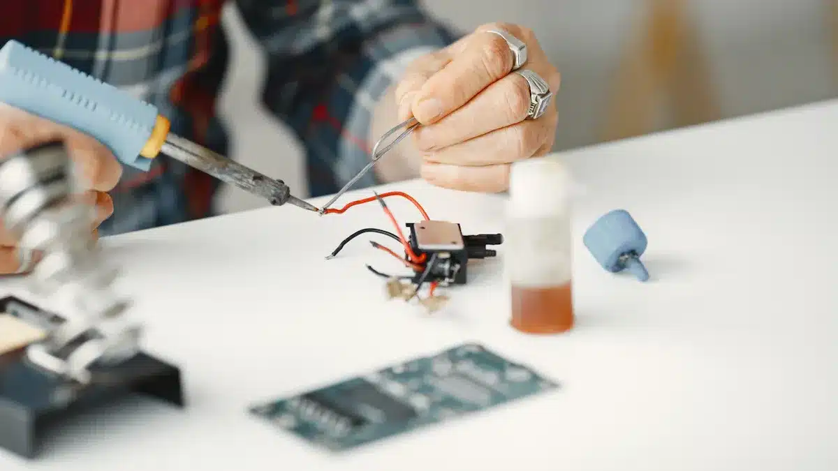
THT Component Insertion
Through-Hole Technology (THT) component insertion is an important step. It helps make circuit boards strong and reliable. You use THT when you need to add big or powerful parts. These parts must handle heat or stress. This step happens after you solder and check surface mount parts.
Manual Insertion
Manual insertion means you put each part in by hand. You push the leads of resistors, capacitors, or connectors into the holes. This way works well for test boards or small batches. You can fix mistakes and make changes if you need to. Manual insertion lets you be flexible, but it takes more time and skill. You must be careful not to bend or break the leads. People can make mistakes, like putting parts in wrong or breaking them.
Here is a table with some main points:
Aspect | Manual THT Insertion |
|---|---|
Cost | Lower upfront investment |
Speed | Slower, labor-intensive |
Volume Suitability | Best for prototyping and low-volume production |
Error Rate | Prone to human errors |
Flexibility | High for small runs and changes |
Mechanical Bond Strength | Strong |
Rework and Repair | Easier due to manual handling |
Tip: Manual insertion saves money for small jobs. It also helps you test new ideas fast.
Automated Insertion
Automated insertion uses machines to put in THT parts. You load the parts into the machine. The machine pushes the leads through the holes quickly and accurately. This way is best for making many boards at once. Using machines lowers mistakes and keeps the process fast. You get fewer bent leads and less broken parts. Automated insertion costs more because you need special machines. It is harder to make changes once you start.
Here is a quick comparison:
Automated insertion is faster and more steady than doing it by hand.
Machines help lower mistakes and make better boards.
You need to spend more money on equipment at first.
Automated lines work best when you make lots of the same board.
THT assembly gives you strong bonds and holds big parts well. You pick manual or automated insertion based on your project size, money, and how much you need to change things.
Wave Soldering
Soldering Process
Wave soldering helps you connect through-hole parts to your PCB fast. You move the board over a wave of hot, melted solder. This step makes strong joints for many pins at once. You must control some key things to get good results:
Put your parts so they do not block each other. Turn them sideways to the wave for even solder.
Keep the wetting angle under 30°. Clean boards and the right flux help the solder spread.
Set the solder wave heat between 250°C and 270°C. Move the conveyor at 1.5–2.5 meters per minute. This keeps the board in the solder for 2 to 4 seconds. It stops weak or brittle joints.
Use flux to help the solder flow better. Flux lowers surface tension and helps the solder reach every joint.
Warm up your PCB before soldering. This stops thermal shock. For single-sided boards, use 90–100°C. For double-sided, use 100–110°C. For multilayer boards, use 115–125°C.
Cool the board slowly after soldering. Slow cooling stops warping and keeps joints strong.
Tip: Always check the solder heat and conveyor speed. Even small changes can change how good the joints are.
Quality Checks
After wave soldering, you must check your boards to make sure every joint is strong. Use these steps to keep your assembly quality high:
Make sure you used the right solder and flux for your board.
Test the bath and zone heat, even when it is hard, to make sure joints form well.
Check and set the conveyor speed. If it is too fast or slow, you can get weak or extra solder.
Make sure your workers have the right training and certificates.
Use process flow charts and risk checks to find and fix problems.
You should also use different ways to check for defects:
Description | Defects Detected / Purpose | |
|---|---|---|
Visual Inspection | People or machines look at solder joints and part placement | Finds missing solder, bridges, or wrong parts |
Automated Optical Inspection (AOI) | Fast cameras check how solder joints look and where parts are placed | Finds too much or too little solder, bridges, bad joints |
X-ray Inspection | Looks inside parts to check hidden solder joints | Finds empty spots, bad solder shapes, hidden problems |
In-Circuit Testing (ICT) | Electrical probes test for shorts, opens, and part values | Finds faults from bad soldering |
Process Parameter Control | Watches solder type, flux, heat, wave height, and speed | Keeps the process and joints the same quality |
Operator Qualification | Training and certificates for workers | Lowers mistakes and keeps standards high |
Statistical Process Control | Uses data to watch and control the soldering process | Keeps quality steady and finds problems early |
Functional Testing | Tests the finished PCB to see if it works right | Checks if the board works and if solder joints are strong |
Note: Careful checks after wave soldering help you find problems early and keep your product quality high.
Final PCBA Inspection
Functional Testing
You need to make sure your assembled PCB works as expected before you ship it. Functional testing checks if your board does what it should in real-world conditions. You connect the board to power and run it through its normal tasks. This step helps you find problems that earlier inspection steps might miss.
The main objectives of final inspection include:
Preventing batch defects by catching issues early.
Confirming that all components are in the right place and facing the correct way.
Verifying that the board meets all technical and customer requirements.
Checking for any leftover flux or contamination.
Making sure the board follows industry standards like IPC-A-610.
Allowing only boards that pass inspection to move forward.
You use tools like Automated Optical Inspection (AOI), X-ray inspection, and In-Circuit Testing (ICT) to spot missing parts, soldering problems, or misaligned components. These methods help you confirm that your board is ready for use and meets all quality standards. Good inspection programs also track data and use sample rates to keep quality high.
Tip: Always mark and record your inspection results. This helps you avoid delays and keeps your production on track.
Burn-In Testing
Burn-in testing pushes your board to its limits. You run the PCB at high and low temperatures, different voltages, and sometimes for days at a time. This process helps you find hidden problems that might not show up during normal testing.
Burn-in testing detects early failures by stressing the board with heat, voltage, and power cycles.
You can spot defects like weak solder joints, bad components, or firmware errors.
The test usually lasts from 12 to 168 hours, depending on your needs.
Burn-in testing helps you measure reliability and predict how long your board will last.
You reduce warranty claims and customer returns by catching problems before shipping.
You use burn-in testing to make sure your product meets client expectations and industry standards. This step gives you confidence that your boards will work well in the field and helps protect your reputation.
Note: Burn-in testing is a key part of quality control. It helps you deliver reliable products and avoid costly repairs later.
Cleaning and Final Assembly
Cleaning Methods
You need to clean your PCB after the main assembly steps. This helps you remove solder balls, flux, dust, and other debris. Clean boards last longer and work better. Industry standards like IPC-5704 and IPC-J-STD-001 set rules for how clean your board should be. If you leave residues, you risk corrosion or electrical shorts. You want to meet these standards to ensure long-term reliability and final quality control.
Follow these steps for the best cleaning results:
Inspect your board for flux, dust, or grease. Check what type of flux you used.
Gather your tools: high-purity isopropyl alcohol, anti-static brushes, lint-free wipes, compressed air, and gloves.
Blow off loose debris with compressed air. Use a soft brush for stubborn spots.
For manual cleaning, dip your brush or wipe in alcohol. Gently scrub away flux and grease.
Wipe the board with a dry, lint-free cloth.
Dry the PCB in a dust-free area or use low heat for a few minutes.
Inspect under a magnifier. Clean again if you see any residue.
Test the board to make sure there are no shorts or open circuits.
Tip: Clean your board soon after soldering, usually within 24-48 hours. This helps you avoid hard-to-remove residues.
Mechanical Assembly
Mechanical assembly is the last step before you finish your product. You place the PCB into its enclosure, which can be plastic or metal. Secure the board with screws or clips. Connect wires or cables to other parts of your device. These connections let your board send power and data where needed.
You need skilled workers and the right tools for this step. Good mechanical assembly keeps your board safe and working well. Quality checks during final assembly make sure your product meets all standards. You want to check that every connector and wire is in the right place. Contract manufacturers often help with this stage to save you time and money.
Step | What You Do | Why It Matters |
|---|---|---|
Place PCB in case | Fit the board into the enclosure | Protects the board |
Secure with screws | Fasten the board with screws or clips | Stops movement |
Connect wires | Attach cables or connectors | Enables communication |
Inspect assembly | Check all parts and connections | Ensures quality |
You finish the final assembly by checking everything one last time. This step helps you deliver a reliable product to your customer.
Packaging and Shipping
Protective Packaging
You have to keep your finished PCBs safe when you ship them. Good packaging stops damage from static, water, or bumps. If you pick the right materials, your boards are less likely to get hurt or sent back.
Here are some common ways to protect your boards:
Tissue Paper and Bubble Wrap: Use these for simple boards that do not need much protection.
Pink Poly Bags and Bubble Wrap: These help stop static and give soft padding.
ESD Bags: These shiny silver bags with Ziploc seals keep static away from sensitive parts.
Moisture Barrier Bags: These sealed bags with drying packs keep water out. They work well for shipping by sea or to wet places.
Vacuum Sealed Packaging: This takes out air and water for very sensitive boards. You can use this with ESD bags.
Conductive Corrugated Cardboard: This is a cheap choice for short trips.
Conductive Fluted Plastic: This is strong and keeps out water, good for long or repeat shipping.
Injection Molded Plastic Containers: These are tough boxes for storing and using again.
Anti-Static Foam Interiors: Pink foam or special inserts keep the board safe and stop static.
Black Conductive PCB Shipping Boxes: These boxes have locking flaps and anti-static foam for extra safety.
Tip: Always use anti-static packaging for boards with sensitive chips. Moisture-proof and anti-vibration packaging help stop rust and damage.
Documentation
You need to send the right papers with your shipment. Good paperwork helps you avoid mix-ups and delays. It also shows your boards meet quality rules.
Here is a checklist for shipping papers:
Bill of Materials (BOM): Lists all parts with details like part number and quantity.
Gerber Files: Shows the PCB layers, solder mask, and drill holes.
Pick and Place File: Tells where each part goes and how it faces.
Assembly Drawings: Gives visual guides for placing and turning parts.
Assembly Instructions: Lists steps, soldering rules, and cleaning needs.
Assembly Layer File: Good for boards with many layers.
Sample or Reference Board: Not required, but helps with new builds.
Quantity and Delivery Timeline: Says how many boards and when to send them.
Certification and Quality Standards: Shows your boards follow industry rules.
Extra Recommendations: Use version control, clear file names, and add contact info.
Note: Put ESD warning stickers, drying packs, and anti-static tape in your packaging. These small things help keep your boards safe and make customers happy.
Step-by-Step Guide Recap
Key Takeaways
You have learned how to move from design to finished pcba. The pcba manufacturing process starts with careful planning and design checks. You gather all your files and review your bill of materials. Next, you source parts and check their quality. You clean your boards and make stencils for solder paste. You use stenciling and inspection to prepare for surface mount assembly. Pick and place machines set parts on the board with high accuracy. Reflow soldering creates strong joints. You inspect each board using visual checks, AOI, and X-ray. In-circuit testing helps you find hidden problems. You insert through-hole parts by hand or with machines. Wave soldering connects these parts. You finish with functional and burn-in testing. Cleaning and mechanical assembly come next. You package your boards and include all needed documents. Each step helps you meet quality standards and avoid mistakes.
Best Practices
You can follow some best practices to get the best results in pcba. Always start with clear design files and a complete BOM. Use trusted suppliers for parts. Check every part before you use it. Clean your boards before and after assembly. Use the right tools for stenciling and placement. Calibrate your machines often. Inspect your boards at every stage. Test your boards with both in-circuit and functional tests. Use burn-in testing for extra reliability. Clean your boards after soldering. Protect your boards with good packaging. Keep records of every step. When you work on prototyping, follow the same steps as in full manufacturing. This helps you find problems early. Prototyping lets you test your design before large-scale assembly. You can improve your process and meet quality standards every time.
Tip: Treat prototyping as a full production run. This habit helps you build reliable pcba and keeps your workflow strong.
You can achieve better pcba results when you follow a clear, step-by-step process. Careful inspection at each stage helps you catch mistakes early and build reliable boards. Use best practices to avoid common problems in your pcba projects. Try these steps in your next build for stronger results. If you want to learn more, check out guides from IPC or watch online tutorials for extra tips.
FAQ
What is the difference between SMT and THT?
SMT places parts on the surface of the board. THT puts part leads through holes in the board. SMT works best for small parts and fast assembly. THT gives stronger connections for big or heavy parts.
How do you prevent soldering defects?
You use clean boards, the right solder paste, and well-calibrated machines. You check the temperature profile during reflow. You inspect each board after soldering. These steps help you avoid weak joints and bridges.
Why is cleaning the PCB important after assembly?
Cleaning removes flux, dust, and other debris. If you skip this step, you risk corrosion and short circuits. Clean boards last longer and work better in real use.
How do you know if a PCB passes inspection?
You check for missing parts, bad solder joints, and correct placement. You use tools like AOI, X-ray, and ICT. If the board meets all standards and works in tests, it passes inspection.
What documents should you include when shipping PCBs?
You should include the Bill of Materials, Gerber files, assembly drawings, and test reports. These documents help your customer check quality and build or repair the board if needed.
See Also
Detailed Walkthrough Of The PCBA Production Process
Complete Overview Of The Steps In PCBA Manufacturing
Key Stages In The PCBA Production Workflow Explained