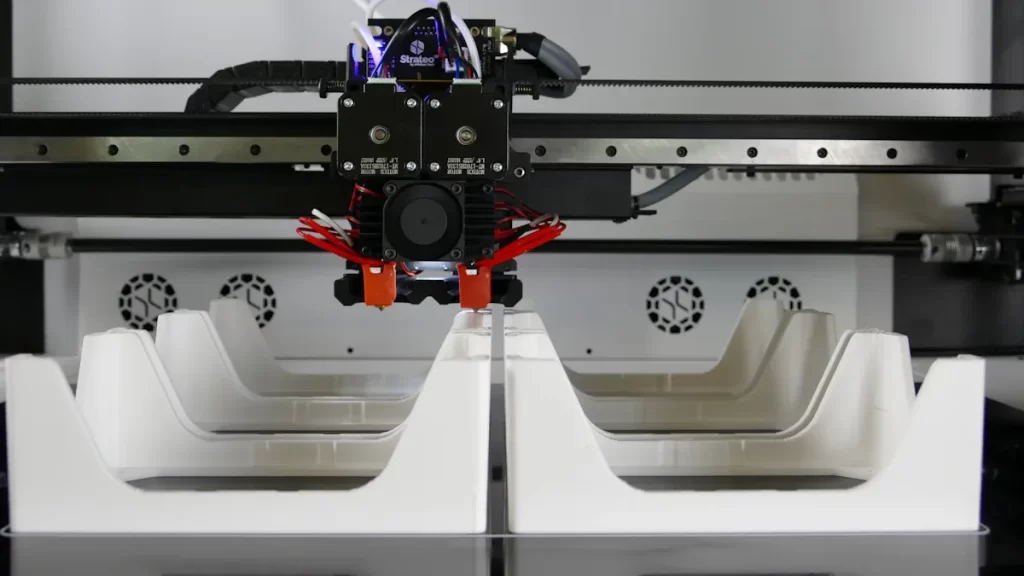
PCBA manufacture involves placing electronic components onto a circuit board, which is essential for creating functional electronic devices such as phones and medical equipment.
Understanding the steps involved in PCBA manufacture highlights the precision and care required in the process. For example, the global PCB market is projected to expand from $68.4 billion in 2023 to $105.8 billion by 2032, driven by sectors like automotive and healthcare. This growth underscores the demand for more advanced and reliable PCBs.
Each phase of the PCBA manufacture process ensures that the final product adheres to stringent quality standards. For instance, the solder resist layer must remain within ±0.15mm. These standards are crucial for ensuring that devices are durable and perform effectively, making this process vital for both manufacturers and consumers.
Key Takeaways
Knowing the PCBA process is important for making good electronics. Every step, from planning to testing, ensures quality and works well.
A clear Bill of Materials (BOM) is very important. It prevents errors and keeps production easy by ordering correct parts.
Tests like Automated Optical Inspection (AOI) and X-ray find issues early. This saves money and makes the product more reliable.
Picking the right assembly method, like Surface Mount Technology (SMT) or Through-Hole Technology (THT), affects speed and connection strength.
Good packaging and shipping keep PCBs safe from harm. Strong materials and careful packing make sure boards arrive safely.
Design and Preparation in PCBA Manufacture
PCB Design and Layout
Every successful PCB starts with a good design. This design shows where parts go and how they connect. It makes sure the board works well and fits the needed size. Over time, PCB designs have changed a lot:
1897: Electronic tubes were invented, starting modern electronics.
1925: Charles Ducas printed circuit patterns on materials.
1948: The U.S. began making PCBs for businesses.
Today, smaller devices and IoT are shaping the industry. Multi-layer boards pack more features into tiny spaces. IoT-ready PCBs include Wi-Fi and Bluetooth for smart devices. These changes help PCBs keep up with new technology.
Bill of Materials (BOM) Creation
A BOM lists all parts needed for making a PCBA. It helps with buying and building. A correct BOM avoids mistakes and keeps production smooth.
A good BOM stays updated. If designs change, the BOM updates too. This ensures the right parts are ordered and no old parts are used.
A strong BOM lists part numbers, amounts, and details. It helps manage stock and avoids delays from missing parts. Without a good BOM, costs can rise, and work slows down. This step is very important for success.
Sourcing Components
Getting parts is key to making a PCB. Parts must be high-quality and arrive on time. Buying in bulk and talking with suppliers can save money and fix problems fast.
Description | |
|---|---|
Key Performance Indicators | Check data to see how well sourcing works. |
Bottleneck Identification | Look for problems that slow things down. |
Proactive Communication | Talk to suppliers early to solve issues. |
AI tools now help with sourcing. They predict what parts are needed and stop shortages. Automation checks supplier performance and helps make smart choices. Using these tools makes sourcing easier and keeps production running smoothly.
PCB Manufacturing Process: Fabrication
Substrate Material Preparation
The substrate is the base of a circuit board. It holds parts and keeps electricity flowing safely. Good substrates last long and work well. Things like heat transfer and strength decide if a material is good. Materials like ceramics handle heat better, which is important for powerful devices.
Manufacturers test substrates to ensure they are consistent. For example, they check pH levels using ASTM E70 rules. This stops problems like material breaking down. By following strict checks, defects are avoided, and the substrate works well for making PCBs.
Imaging and Etching
Imaging and etching create paths on the circuit board. These paths connect the parts. The design is copied onto the board, and extra copper is removed. This step needs to be very accurate. For example, lasers can make tiny paths with a width of 0.5 mil.
Special tools check leftover copper to avoid mistakes. They also measure smoothness to keep the board even. Following ISO 4287-1 rules ensures the board is reliable. These steps help prevent errors and make the board work better.
Layer Lamination
Layer lamination sticks layers of the board together. This is needed for boards with many layers used in modern gadgets. Materials must match well during this process. Some need specific heat and pressure to avoid problems.
Problems like bubbles or sliding layers can happen during lamination. To stop this, manufacturers control heat, glue, and thickness carefully. Good lamination keeps layers strong and working under tough conditions. This makes the board last longer and perform better.
Drilling and Plating
Drilling makes small holes in the PCB. These holes, called vias, link layers and hold parts. They help signals move between layers. Advanced machines, like lasers or fast drills, make these holes. The holes can be as tiny as 0.1 mm wide. This accuracy meets modern electronics’ needs.
After drilling, plating adds a metal layer inside the holes. This layer connects the board’s layers electrically. The process cleans the holes, adds copper, and strengthens it with electroplating. Good plating stops problems like weak signals or bad connections. This keeps the PCB working well.
Manufacturers check the holes for mistakes after plating. They look for problems like uneven plating or misaligned holes. By following strict rules, they ensure the PCB works properly in its final use.
Solder Mask and Silkscreen Application
The solder mask protects the PCB and helps with soldering. It covers the board’s surface, leaving only solderable areas open. This stops short circuits during assembly. Some spots, like heat sinks, might not have solder mask due to space limits. Manufacturers carefully apply the solder mask to keep the board working right.
The silkscreen adds labels and marks to the PCB. These marks show where parts go during assembly. Manufacturers make sure the ink doesn’t block pads or mess up soldering. This step makes the board easier to use and reduces mistakes.
Both solder mask and silkscreen steps are important. They make the PCB strong and simple to use. By following industry rules, manufacturers deliver high-quality boards that meet your needs.
PCB Manufacture: Component Placement and Assembly
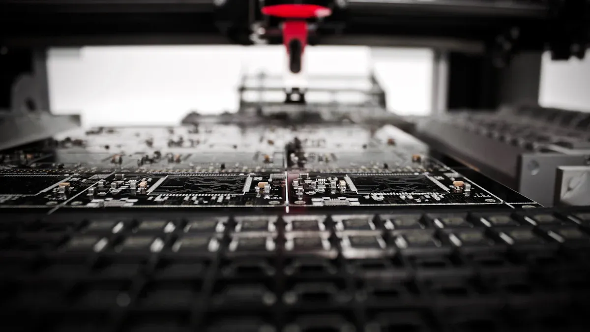
Surface Mount Technology (SMT) Assembly
Surface Mount Technology (SMT) is a common way to assemble PCBs. It places parts directly on the board’s surface without drilling. This method is quick and precise. Using SMT saves time and lowers costs.
Benefits of SMT Assembly:
Faster production: Products are made quickly to stay ahead.
Higher output: More PCBs can be made with the same tools.
Better quality: Machines reduce mistakes and keep results consistent.
Lower expenses: Efficiency cuts down the cost per board.
Modern SMT machines use fast chip placers and smart feeders. These tools make the process accurate and quick, ensuring great results.
Through-Hole Technology (THT) Assembly
Through-Hole Technology (THT) is another way to assemble PCBs. Unlike SMT, THT needs holes drilled into the board for parts. This method makes strong connections, perfect for tough environments.
Reasons to Use THT Assembly:
Strong connections: Great for military and space industries.
Handles heat well: Works for high-power electronics.
Easy to test: Bigger parts are simple to adjust.
High-frequency use: Works well with high-frequency signals.
THT takes more time and effort but is very reliable. It’s a good choice for smaller production runs or special uses.
Soldering Techniques (Reflow and Wave Soldering)
Soldering attaches parts securely to the PCB. Two main methods are reflow soldering and wave soldering.
Reflow soldering melts solder paste with heat to bond parts. Automated systems improve this process by making it more controlled and reliable. These systems ensure the soldering meets quality standards.
Wave soldering is used mostly for THT assembly. A wave of melted solder flows over the board, creating strong bonds. Studies show lead-free wave soldering works well in factories. This method is great for making many boards at once.
Both soldering methods are important for strong and reliable PCBs. Picking the right method helps ensure your final product works perfectly.
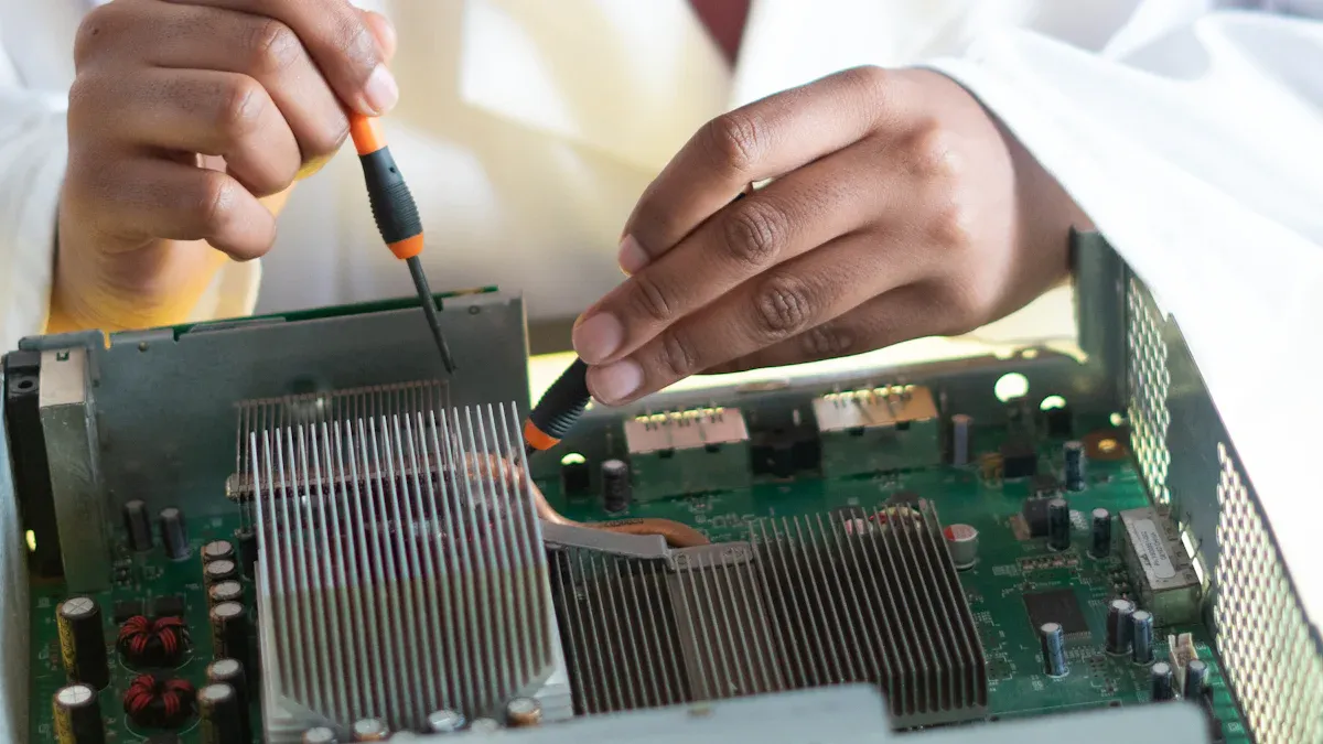
Testing and Inspection in PCBA Manufacture
Testing and inspection are important to make sure PCBs work well. These steps find problems early, lowering failure risks and improving quality. Below are the main testing methods used in making PCBs.
Automated Optical Inspection (AOI)
Automated Optical Inspection (AOI) uses cameras to check PCBs for problems. This method avoids human mistakes and gives steady results. AOI finds issues like missing parts, bad soldering, or misaligned pieces. Catching problems early saves money and speeds up production.
Improvement Type | Description |
|---|---|
Consistency and Repeatability | Keeps checks the same every time, reducing errors. |
High Speed | Checks PCBs faster than people can, boosting output. |
Early Defect Detection | Spots problems early, cutting costs and improving quality. |
Objective Results | Gives clear data, avoiding personal opinions in checks. |
Traceability and Data Analysis | Creates detailed reports to improve processes and quality. |
Modern AOI systems also use AI to study data, making checks even better and faster.
X-Ray Inspection
X-Ray inspection looks inside PCBs without breaking them. It finds hidden problems like cracks, gaps, or misplaced layers. This method creates clear 2D and 3D images to see inside the board.
Benefits of X-Ray Inspection:
Finds hidden solder problems to keep PCBs strong.
Measures sizes and spaces very accurately.
Spots tiny flaws that need fixing for high standards.
Shows why problems happen with detailed internal data.
X-Ray inspection finds issues other methods miss, making products more reliable.
Functional Testing
Functional testing checks if the PCB works as it should in real life. It tests how the system runs and interacts with other parts. This step finds problems early, improving the product’s overall quality.
Key Benefits of Functional Testing:
Confirms the PCB does what users need it to do.
Improves quality by catching problems early.
Makes sure everything works smoothly together.
Functional testing is key to making dependable and high-quality PCBs. By following strict rules, this step ensures the product works as planned.
In-Circuit Testing (ICT)
In-Circuit Testing (ICT) checks if a PCB works correctly. It tests each part and connection on the board. Finding problems early avoids expensive fixes later.
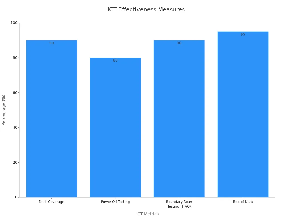
ICT uses smart tools to test parts’ functions. It finds issues like broken circuits, short circuits, or bad soldering. For instance, power-off testing catches 80% of solder problems. Boundary scan testing finds over 90% of faults in complex PCBs. These tests make sure every PCB layer works well.
Test Type | What It Finds |
|---|---|
Fault Coverage | Spots 90% of issues, like short circuits. |
Power-Off Testing | Finds 80% of solder problems. |
Boundary Scan Testing | Detects over 90% of faults in dense PCBs. |
Bed of Nails | Covers 95% of faults, great for large-scale production. |
ICT often uses a “bed of nails” tool. This tool presses pins onto the PCB to check its pathways. It works well, finding up to 95% of faults, especially in big productions. This step ensures the PCB meets quality rules before moving forward.
Adding ICT to your process improves product quality. It ensures all parts and connections work as they should. This reduces defects and makes products more reliable.
Final Steps in the PCB Manufacturing Process
Cleaning and Finishing
Cleaning removes dirt, dust, and oils from the PCB. These can harm how the board works. Special cleaning methods help get rid of these impurities. For example, ultrasonic cleaning uses sound waves to shake off tiny particles. This works well for boards with small, tight spaces. Another method uses deionized water or chemicals to clean the board deeply.
After cleaning, a finish is added to protect the PCB. This layer stops rust and makes the board last longer. Common finishes include gold, silver, or tin. Gold is great for conductivity, while tin is cheaper and still reliable. Picking the right finish helps the PCB work better and stay strong over time.
Packaging and Shipping
Good packaging keeps the PCB safe during shipping. Without it, parts like resistors or coatings can get damaged. Packages might be dropped, shaken, or crushed during transit. These impacts can cause hidden problems that affect the board’s performance. To avoid this, manufacturers use strong materials like foam, anti-static bags, and sturdy boxes.
Using proper packaging reduces the chance of damage. Foam protects the PCB by absorbing shocks. Anti-static bags stop static electricity from harming sensitive parts. Labels like “Fragile” or “Handle with Care” remind handlers to be gentle.
By focusing on good packaging and shipping, the PCB arrives safely. This step ensures the board is ready to use and stays high-quality.
The PCBA process has many important steps. These include design, assembly, testing, and finishing. Each step ensures the PCB works well and meets quality standards. For instance, tests like Automated Optical Inspection (AOI) and X-ray checks find problems early. This stops expensive mistakes later.
Strict quality checks are very important. Even small problems can harm how devices work and their safety.
Industries like aerospace and medical devices need strict quality rules. Careful processes help meet these rules and lower failure rates. Fixing issues early makes products better. By following these steps, you can make strong and reliable PCBs with good parts and layers.
FAQ
What is the difference between PCB and PCBA?
A PCB is just a plain circuit board. It has no parts on it. A PCBA (Printed Circuit Board Assembly) includes the PCB with all its parts attached. The PCBA is ready to use in devices.
Why is testing important in PCBA manufacturing?
Testing checks if the PCBA works properly. It finds problems early, so the final product doesn’t fail. This step makes the product more reliable and saves money over time.
How does SMT differ from THT assembly?
SMT puts parts directly on the board’s surface. It’s faster and costs less. THT needs holes for parts, making stronger connections. SMT is best for big batches, while THT is better for tough or high-power uses.
What materials are commonly used for PCB substrates?
Materials like FR-4 (fiberglass with epoxy) and ceramics are common. These materials are strong, handle heat well, and keep electricity safe. They help the PCB work reliably.
How do manufacturers ensure PCBs are free from defects?
Manufacturers use tools like Automated Optical Inspection (AOI) and X-ray testing. These tools find problems like misplaced parts or cracks. Careful checks make sure the PCB meets quality rules.
See Also
An In-Depth Overview of Steps in PCBA Manufacturing
Understanding the Process and Steps of PCBA Assembly
The Functionality of SMT in PCBA Assembly Process
Investigating Testing Methods for Enhanced PCBA Manufacturing
Strategies to Enhance Workflow Efficiency in PCBA Production