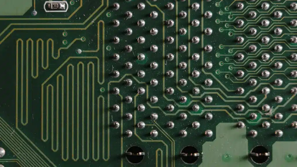
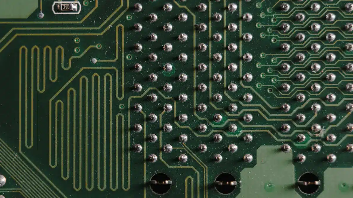
In circuit board design, a circuit board via is very important. It connects different layers of the board. Circuit board vias help signals and power move through the board. Each type of via has a special job. For example, thermal vias control heat in powerful devices. They help heat move away, which stops damage. This also makes the hardware last longer. Knowing these details will help you pick the right circuit board vias for your projects.
Key Takeaways
Learn about the different types of PCB vias. These include through-hole, blind, and buried. This helps you pick the best one for your project.
Think about the size and shape of vias. These things can change signal quality and how well they are made.
Use thermal vias to control heat in powerful devices. This helps them work better and last longer.
Look at the pros and cons of each via type. This helps you make smart choices that fit your design needs.
Use different types of vias in your PCB design. This saves space and improves electrical performance.
Types of PCB Vias
In PCB design, knowing the different types of vias is very important. Each type has a special job and can greatly affect how well your circuit board works. Here’s a look at the main types of PCB vias:
Type of Via | Description |
|---|---|
Through-Hole Vias | Drilled from the top to the bottom layer, connecting all layers of the PCB. |
Blind Vias | Connect outer layers to one or more inner layers, but do not go all the way through. |
Buried Vias | Connect only the inner layers, so they are hidden from the surface. |
Microvias | Very small vias made with lasers, used in HDI boards. |
Stacked Vias | Multiple vias placed on top of each other across high-density layers. |
Staggered Vias | Vias that are not directly on top of each other across layers. |
Tented Vias | Vias covered with a solder mask for protection or to keep them separate. |
Via-in-Pad (VIP) | A via located right under a component pad, often filled and capped. |
Choosing the right type of via for your project is very important. Each type has its pros and cons, which can change costs, how easy they are to make, and how well they work. Here’s a quick comparison of some common types:
Via Type | Advantages | Disadvantages | Cost Range |
|---|---|---|---|
Blind Via | Saves space on the outer layer; reduces signal problems. | More complex and expensive to make; limited connections. | $0.05 – $0.10 per via |
Buried Via | Frees up space on outer layers; improves signal quality. | Costly to make; harder to check or fix. | $0.05 – $0.10 per via |
Through-Hole | Cheapest option; easy to drill. | Not great for high-density designs. | < $0.01 per via |
Microvias | Lowers overall board cost by using fewer layers. | One of the most expensive; needs precise drilling. | $0.10 – $0.20 per via |
Stacked Vias | Allows for many connections in a small space. | Costs can add up; alignment can be tricky. | $0.15 – $0.30 per via |
Via-in-Pad | Reduces overall board size, balancing the cost. | Adds 10-20% to standard via costs because of extra steps. | +10-20% to standard cost |
When you pick a via type, think about how it affects the electrical and mechanical features of your PCB. Here are some important points to remember:
The size of vias can affect how well signals transfer. Properly sized vias help keep signal quality during transmission.
Bigger vias can help with heat loss, making them good for high-power uses and reducing heat problems.
Standard sizes for vias help ensure good production and reliable results.
The choice of materials affects how well vias work, impacting capacitance, inductance, and impedance in high-frequency designs.
By learning about the different types of PCB vias and their uses, you can make smart choices that improve how well your projects work.
Through-Hole Vias
Overview of Through-Hole Vias
Through-hole vias are a basic type of circuit board via. They connect all layers of a PCB by drilling a hole from the top to the bottom. This design makes sure electrical connections between layers are strong. You often see through-hole vias in older PCB designs. They are bigger than other types, which makes them easier to make and check.
Here are some key features of through-hole vias:
Characteristic | Measurement/Requirement |
|---|---|
A ≥ 20mil | |
Minimum distance between hole plate and copper foil | B ≥ 20mil, C ≥ 20mil |
Minimum distance between PTH and hole to outline | D ≥ 20mil |
Recommended minimum distance between NPTH and hole to outline | E ≥ 40mil |
Minimum distance between hole wall and bonding pad | 0.2 mm |
No through holes in extending outward area | 1.5 mm from device metal shell and PCB |
Use Cases for Through-Hole Vias
Through-hole vias are used in many different areas. They are especially good for mounting through-hole parts like connectors and resistors. You can find them in consumer electronics, power supplies, and industrial controls. Here are some common uses:
Signal routing: Through-hole vias are great for routing signals on circuit boards, especially in less crowded designs.
Escape routing: They help route larger surface mount parts.
Power routing: Bigger through-hole vias carry more current, making them good for power and ground connections.
Stitching vias: These vias connect many points to a plane, improving electromagnetic interference (EMI) protection.
Thermal vias: They help remove heat from parts, often needing larger sizes.
Through-hole vias offer a strong solution for many PCB designs. Their features make them a popular choice in many fields.
Blind Vias
Overview of Blind Vias
Blind vias are a special kind of circuit board via. They connect the outer copper layer to one or more inner copper layers. However, they do not reach the bottom layer. This design makes them great for multi-layer printed circuit boards (PCBs). Here are some important features of blind vias:
They are smaller than through vias.
Blind vias often get filled with non-conductive or conductive ink.
They help keep the PCB strong by reducing the number of drilled holes.
These features make blind vias a popular choice in high-density interconnect (HDI) applications. They save space by connecting certain layers without affecting others. In fact, blind vias can cut the overall board size by 20-30%. This compact design allows for better layouts and improves signal quality by shortening signal paths. Shorter paths reduce signal reflection and crosstalk, which is very important for high-performance uses.
Use Cases for Blind Vias
Blind vias are used in many areas because of their unique benefits. Here are some common uses:
Smartphones: They help create thin boards with complex circuits.
Wearables: Their tight design supports flexible layouts.
Medical devices: They provide small, precise, and reliable connections.
Military and aerospace: High performance in small spaces is very important.
HDI PCBs: They allow for more signals in a small area.
Buried Vias
Overview of Buried Vias
Buried vias are special types of circuit board vias. They only connect the inner layers of a PCB. They do not reach the outer layer. This makes buried vias great for complex multilayer boards. They help save space and improve performance in crowded designs.
Here are some key features of buried vias:
Characteristic | Detail |
|---|---|
No | |
Connects Inner Layers | Yes |
Manufacturing Complexity | High |
Buried vias need careful manufacturing methods. Their complexity can lead to higher production costs. But, the benefits they offer can be worth these costs in many cases.
Use Cases for Buried Vias
Buried vias are important in many applications. Here are some common uses:
High-Density Interconnect (HDI) Designs: Buried vias help save space in small devices like smartphones and tablets.
Enhanced Performance in Multilayer Boards: They improve signal quality in fast circuits by shortening signal paths, which is important for RF uses.
Design Flexibility and Optimization: Buried vias allow for complex routing without changing surface layouts, helping manage signals better.
You will often find buried vias in advanced electronics, where space and performance matter a lot. Their ability to connect inner layers without affecting the outer layer makes them a popular choice for engineers designing modern PCBs.
Microvias
Overview of Microvias
Microvias are very small holes in printed circuit boards (PCBs). They connect different layers of the board. Their diameters can be as tiny as 0.004 inches. This size is much smaller than regular vias. Because they are smaller, you can fit more connections on the board. According to IPC-T-50M, a microvia is a blind structure. It has a maximum aspect ratio of 1:1 and a depth of no more than 0.25mm. Vias with diameters less than 150 microns are microvias. They have benefits like lower resistance compared to regular vias. This helps them handle faster speeds and larger amounts of data. This improvement is very important for today’s PCB uses.
Microvias are key for high-density interconnect (HDI) PCB designs. They allow for more connections in a smaller space, which is important for making devices smaller. Here are some main benefits of microvias in HDI designs:
They improve electrical performance by shortening paths for signals.
They lower parasitic capacitance and inductance, which is important for fast applications.
They help add more layers without making the PCB bigger.
Stacked vs. Staggered Microvias
When using microvias, you can choose between stacked and staggered types. Each type has its own benefits and challenges.
Stacked microvias need more steps to make, which makes them more complex. They can create a compact design but may cause reliability issues in some situations.
Staggered microvias are better for reliability and yield, especially in tough conditions. They are preferred in designs that experience a lot of thermal cycling because they reduce stress on the via walls.
Choosing the right type depends on your design needs and where the PCB will be used. Knowing these differences can help you make better choices for your projects.
Thermal Vias
Overview of Thermal Vias
Thermal vias are very important for controlling heat in printed circuit boards (PCBs). They help heat escape from parts that use a lot of power. This keeps devices working safely and well. Thermal vias connect hot parts to bigger copper areas or heat sinks. This helps heat move away better.
Here are some key functions of thermal vias:
Function of Thermal Vias | Description |
|---|---|
Enhance Thermal Conductivity | Thermal vias help heat move away from parts. |
Reduce Thermal Resistance | More thermal vias lower the overall thermal resistance of the PCB. |
Aid in Heat Distribution | They help spread heat evenly, stopping hot spots. |
Applications of Thermal Vias
You can find thermal vias in many electronic devices where managing heat is very important. Here are some common uses:
Point-of-Sale Terminals: These devices deal with many transactions, creating heat from processors and power circuits.
Digital Signage: They need good heat management to avoid overheating during long use.
Inventory Scanners: These devices stay stable while processing data in tight spaces with little airflow.
To make thermal vias work better, follow these best practices:
Use big groups of vias right under high-power parts.
Use several small vias (0.2–0.3 mm wide) to increase density.
Choose filled vias or via-in-pad designs for better heat transfer.
Also, make sure thermal vias connect to internal ground planes with a solid copper link. This helps heat move away and improves overall performance.
By knowing how important thermal vias are, you can design PCBs that manage heat well. This ensures your electronic devices are reliable and last longer.
Design Considerations
Aspect Ratios
Aspect ratio is very important for making and using vias in your PCB designs. It is the ratio of a via’s depth to its diameter. Keeping the right aspect ratio helps avoid problems during the PCB assembly process. High aspect ratios can cause issues like voids or incomplete plating, which can weaken connections.
Here are the recommended aspect ratios for different via types:
Via Type | Recommended Aspect Ratio | Notes |
|---|---|---|
Through-Hole Vias | 6:1 to 8:1 | IPC reliability standards say this range is needed. An 8:1 aspect ratio is a must for manufacturers. |
Microvias | 1:1 | This is the maximum aspect ratio for laser drilled microvias according to IPC-T-50M. |
High Density Interconnect (HDI) | 10:1 to 12:1 | Some manufacturers can achieve this, but it needs careful design. |
For the best results, keep the aspect ratio of microvias at 1:1 or less. For standard blind and buried vias, keep it below 8:1. This helps ensure good copper deposition and avoids weak connections.
Reliability Factors
When choosing via types for high-performance or important PCB applications, think about several reliability factors:
Optimize Via Design: Make stacked vias with aspect ratios below 1:1. This reduces stress during drilling and plating.
Use Simulation Tools: Use thermal and mechanical simulation tools. These tools help predict how vias will behave under stress, cutting down design changes.
Implement Robust Manufacturing Processes: Make sure drilling and plating are precise to avoid defects. Advanced methods like laser drilling improve reliability.
Adopt Industry Standards: Follow standards like IPC-6012 and IPC-TM-650. These standards help keep quality and performance in via design and testing.
Conduct Reliability Testing: Do thermal cycling tests. These tests mimic real conditions and find possible reliability problems.
Different applications have their own design needs. For example, consumer electronics focus on being small and cost-effective. On the other hand, industrial applications care more about reliability and thermal management. Aerospace applications need to follow strict standards and be very tough.
By knowing these design considerations, you can create PCBs that work well in different situations. This knowledge helps you make smart choices about the types of vias to use in your projects.
Choosing the right type of circuit board via is very important for your PCB projects. Each type of via has a special job and affects how well your design works. Here are some key points to think about:
Know what your design needs, like layout and signal quality.
Look at how many layers and connections you have for the best links.
Pick the right via types for your needs, like through-hole for general use and blind or buried for tight designs.
Check manufacturing limits to make sure it is possible and affordable.
By learning about the features and uses of each via type, you can improve your PCB design. Well-designed vias help keep signal quality, lower interference, and save space. Make smart choices to help your projects succeed.
FAQ
What is a PCB via?
A PCB via is a tiny hole that connects layers of a printed circuit board. It lets electrical signals and power move between layers, making the board work better.
Why are thermal vias important?
Thermal vias help remove heat from parts that use a lot of power. They link hot areas to bigger copper parts or heat sinks, keeping devices safe and working well.
How do I choose the right via type?
Think about what your design needs, like how many layers and signal quality. For general use, through-hole vias are good. For smaller designs, choose blind or buried vias.
What is the difference between stacked and staggered microvias?
Stacked microvias sit directly on top of each other, while staggered microvias are shifted. Staggered microvias usually offer better reliability and lessen stress during temperature changes.
Can I use multiple via types in one PCB?
Yes, you can mix different via types in one PCB design. This method helps you improve performance and save space based on what each part of the board needs.
See Also
Understanding Key Differences Between PCB And PCBA Designs
Choosing The Right PCB Prototype Manufacturer For Your Needs
In-Depth Comparison Of PCBWay And Competing PCB Makers