
A PCB stands for printed circuit board and is very important in electronics. It connects different electronic parts with special paths, helping devices work well. Knowing what PCB stands for is key for anyone interested in electronics. Learning about PCBs helps you understand how they contribute to the design and function of complex devices like smartphones and computers. The growth of PCBs has changed how things are made, making it easier to create small and reliable electronic systems.
Key Takeaways
A PCB, or printed circuit board, connects electronic parts. It helps devices work well.
PCBs use materials like fiberglass and copper paths. These make strong boards that resist heat and carry electrical signals.
There are three main types of PCBs: single-sided for simple devices, double-sided for more complex circuits, and multi-layer for high-performance electronics.
PCBs are important in many areas. They include consumer electronics, industrial machines, and medical devices. They help improve performance and reliability.
Designing and making PCBs needs careful planning. It uses software tools and precise steps to ensure quality and function.
What PCB Stands For
PCB means printed circuit board. This important part is the main support for most electronic devices. A printed circuit board connects different electronic parts. This helps them work together smoothly.
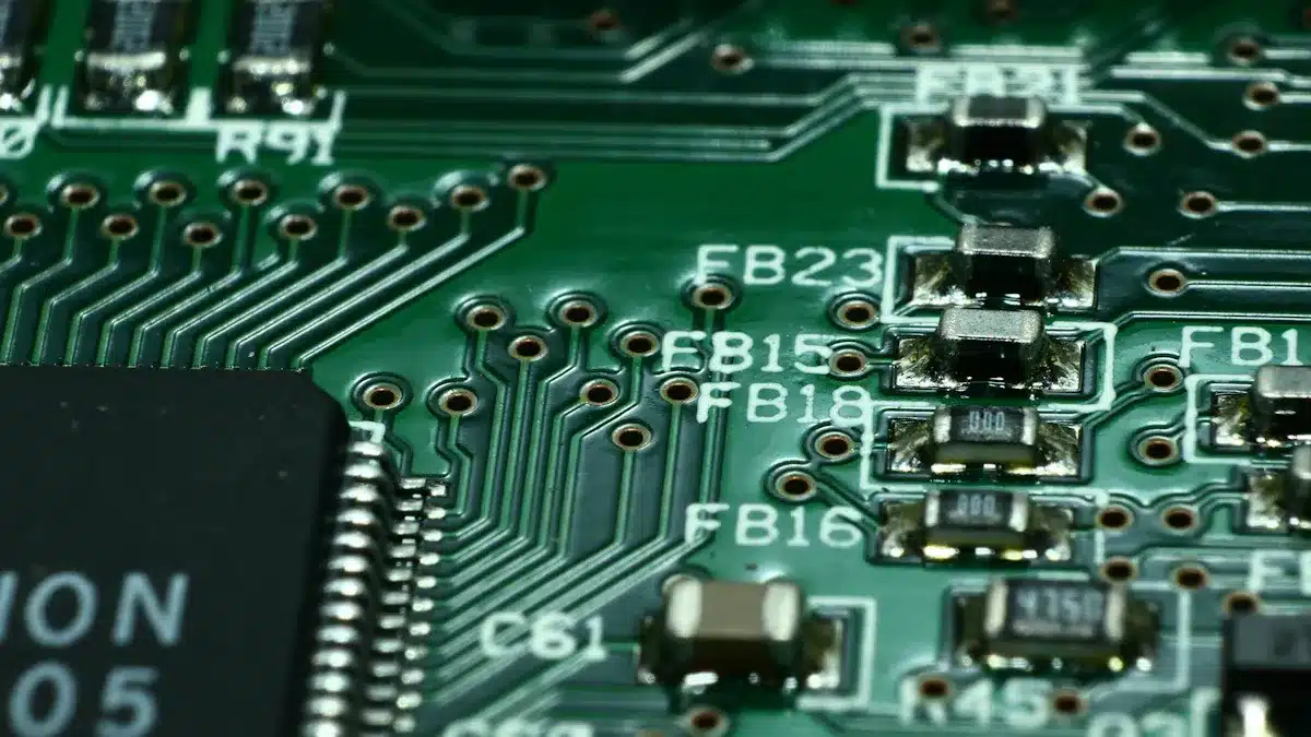
You can picture a PCB as a flat board made from materials that do not conduct electricity, like fiberglass. It has copper paths on its surface. These copper paths work like wires, linking parts like resistors, capacitors, and integrated circuits. By making these connections, PCBs let electrical signals move between parts. This helps the device work properly.
The job of a PCB in electronics is very important. Here are some main jobs of a printed circuit board:
Mechanical Support: PCBs give a strong base for holding electronic parts. This strength helps stop damage when in use.
Electrical Connections: They make paths for electrical signals. This lets parts work together as planned.
Heat Dissipation: PCBs help control heat by moving it away from sensitive parts. This keeps them working well.
Complex Circuitry: The layered design of PCBs allows for detailed circuit layouts. This makes it possible to fit many parts in a small area.
Structure of a Printed Circuit Board
A printed circuit board (PCB) is made of important materials. These materials work together to create a strong base for electronic parts. The most common material in PCBs is FR-4. This is a fiberglass-reinforced epoxy resin. It gives great strength and stops electricity from passing through. It also resists fire and is cheap, so it is used a lot in the industry.
Here’s a quick look at some materials used in making PCBs:
Material | Description | Key Properties and Uses |
|---|---|---|
FR-4 | Fiberglass-reinforced epoxy resin | Strong, stops electricity, fire-resistant, cheap; most common material used. |
Polyimide | Flexible polymer substrate | Stays stable in heat, flexible; mainly used for flexible PCBs. |
Rogers | Polymer-ceramic composite | Great electrical and heat properties; used in high-frequency, high-performance devices. |
Metal Core | Aluminum or copper substrate | Helps manage heat for high-power devices; gives strength and helps with heat loss. |
Copper | Conductive material forming circuit pathways | Needed for electrical flow in PCB paths. |
Copper is very important for how a PCB works. It makes the paths that connect parts like resistors, capacitors, and integrated circuits. These paths act like roads, letting electrical signals move easily across the board.
PCB paths are made on a non-conductive base, creating routes for electric signals. The design of these paths is very important. You need to think about their width, spacing, and layout. This ensures they can handle the needed current without getting too hot or causing problems. Wider paths can carry more current with less resistance. Proper spacing helps reduce interference between signals.
To attach parts to the PCB, pads provide copper spots for soldering. This connection makes sure there is both electrical flow and stability. The careful layout of paths and pads allows for complex circuits, making electronic devices smaller.
Overall, the structure of a PCB mixes different materials and designs to create a strong base for modern electronics. Knowing this structure helps you see how PCBs improve the performance and efficiency of electronic devices.
Types of Circuit Boards
When you look at printed circuit boards (PCBs), you will see three main types: single-sided, double-sided, and multi-layer PCBs. Each type has its own special features and uses.
Single-Sided PCB
A single-sided PCB has one copper layer on one side of a base. You will find parts placed on the other side. This simple design makes it great for basic electronic devices. Here are some important features:
Cost-Effective: Single-sided PCBs are cheaper to make.
Simplicity: They are easy to design and create.
You can find single-sided PCBs in many areas, such as:
Sector | Applications and Examples |
|---|---|
Home appliances, calculators, storage devices, power supplies | |
Automotive | LED lighting boards, radio systems, LED drivers |
Industrial | Devices with less strict specs, RF devices for wireless sensors |
Double-Sided PCB
Double-sided PCBs have copper layers on both sides of one base. This design allows for more complex circuits. You can connect the layers using holes called vias. Here are some benefits:
More ways to route electrical signals.
Better signal quality due to improved layout options.
You will see double-sided PCBs in advanced uses like computer motherboards and communication devices. They support more detailed designs than single-sided boards.
Multi-Layer PCB
Multi-layer PCBs have three or more copper layers stuck together with insulating layers. This design allows for high circuit density and complex layouts. Here are some advantages:
Enhanced Design Flexibility: You can make compact circuits with fast signals.
Improved Signal Integrity: Multi-layer designs lower electromagnetic interference (EMI).
Higher Component Density: Fit more parts without making the board bigger.
These PCBs are important in high-performance devices like smartphones and medical equipment. Their ability to control heat and keep signal quality makes them perfect for modern electronics.
Applications of PCBs
Printed circuit boards (PCBs) are very important in many industries. They connect and support electronic parts, making them essential in today’s technology. Let’s look at some main uses of PCBs.
Consumer Electronics
In consumer electronics, PCBs are the main support for devices like smartphones, laptops, and tablets. They provide a small platform that holds and connects electronic parts through special pathways. This design helps fit more parts into smaller spaces. PCBs allow for important features like touchscreens, Wi-Fi, and cameras. They also help manage power and protect sensitive parts from heat and interference. Because of this, PCBs are key to how modern consumer devices work.
Industrial Use
PCBs are crucial in industrial automation and control systems. They are the base for controlling machines, managing energy, and running automotive assembly lines. Special types of PCBs, like flex and metal core boards, handle heat and vibration better, improving durability and performance. PCBs allow for real-time monitoring and accurate machine operation, which is important for keeping manufacturing efficient. Using advanced materials and technologies in PCBs helps make industrial automation smarter and more sustainable.
Medical Devices
In the medical field, PCBs must follow strict safety and reliability rules. They use strong materials to ensure patient safety, especially in devices that go inside the body. PCBs support important functions in medical equipment, like checking vital signs and controlling imaging devices. Their careful design helps keep signals clear and manage heat, which is vital for how well devices work. Following safety standards makes sure that PCBs in medical devices are safe and effective, making them important for healthcare progress.
Overall, PCBs are essential for how different industries work, helping create new and efficient technologies.
PCB Design and Manufacturing
Designing a printed circuit board (PCB) has several important steps. You need to follow a clear process to make sure your design works well. Here’s how the PCB design process goes:
Develop Library CAD Parts: First, create the symbols and footprints for the parts you will use.
Create the Schematic: Put the symbols on the schematic and connect them with nets to show electrical links.
Simulate the Circuitry: Check if your design works using simulation tools.
Perform PCB Layout: Place the component footprints on the PCB layout based on your design.
Route Traces and Planes: Connect the parts by routing traces and planes, following design rules.
Generate Manufacturing Drawings: Finally, make output files for production, including drawings.
You can use different software tools to help with PCB design. Here’s a table of some popular tools and their features:
Software Tool | Key Features | Pros | Cons | Best For |
|---|---|---|---|---|
Altium Designer | 3D view, supply chain integration | Powerful features, big library | High cost, hard to learn | Professional PCB designers |
EAGLE | Schematic and PCB layout editor | Easy to use, affordable | Limited 3D view | Beginners and mid-level designers |
KiCad | Open-source, 3D viewer | Free, good community support | Limited technical help | Hobbyists, students |
OrCAD | Simulation, signal quality checks | Very precise, many tools | Expensive, complex interface | Advanced engineers, industry pros |
Proteus | Circuit simulation | Great simulation, user-friendly | Only 2D layout | Educators, prototyping designers |
EasyEDA | Web-based, cloud teamwork | Free, collaborative, supplier integration | Limited offline use | Beginners, hobbyists, teams |
After you finish the design, the manufacturing process starts. This process has several steps to make sure your PCB is made correctly:
Design Review and DFM Check: Make sure your PCB design can be made and has no mistakes before production.
Printing Films: Create photo-negative films of each PCB layer using special printers.
Registration: Align films using punched holes for accurate layer matching.
Photoresist Application and UV Exposure: Coat the laminate with photo-reactive resist and expose it to UV light through films to harden the right circuit areas.
Etching: Remove unprotected copper to create circuit traces.
Laminate and Copper Bonding: Add copper foil to the substrate to form the PCB base.
Inner Layer Treatment: Apply etch resist to inner layers before etching to protect copper traces.
Quality control is very important during manufacturing. Techniques like solder paste inspection and automated optical inspection help find problems early. These steps improve reliability and make sure everything meets industry standards.
By learning about the PCB design and manufacturing processes, you can create effective and reliable circuit boards for many uses.
In short, printed circuit boards (PCBs) are very important in today’s electronics. They give support, connect electricity, and manage heat for many devices. PCB technology has changed a lot. This change has made designs smaller and more complex. It helps improve consumer electronics, industrial uses, and medical devices.
Looking ahead, we see new trends like smaller sizes, flexible designs, and using AI in making PCBs. These changes will keep changing the electronics world, making devices better and greener.
Knowing about PCBs is key for anyone who likes electronics. They are the main part of modern technology. 🌟
FAQ
What does PCB stand for?
PCB means printed circuit board. It is the base for most electronic devices. It connects different parts to help them work well.
How is a PCB made?
Making a PCB involves several steps. These steps include design, printing, etching, and assembly. Each step makes sure the circuit board works well and is reliable.
What is the difference between PCB and PCBA?
PCB is the printed circuit board itself. PCBA means printed circuit board assembly. PCBA includes the PCB and all the parts that are soldered on it.
Why are PCBs important in electronics?
PCBs are very important because they give support and connections for parts. They help control heat and allow for complex circuits in devices.
Can I design my own PCB?
Yes, you can design your own PCB with different software tools. Many programs have easy-to-use interfaces that help you create good designs for your projects.
See Also
Understanding PCBA And Its Function In Electronics
Defining PCBA And Its Importance Within Electronics
Explaining What PCBA Means And Its Purpose