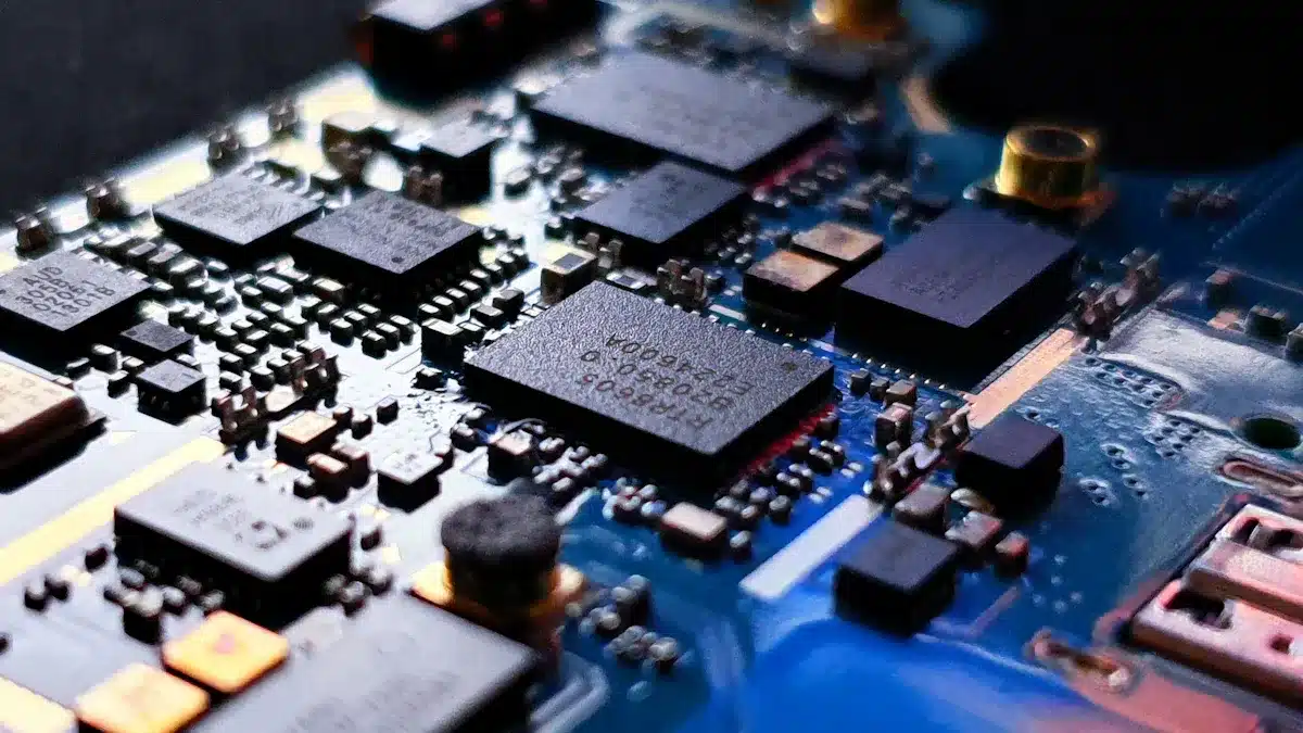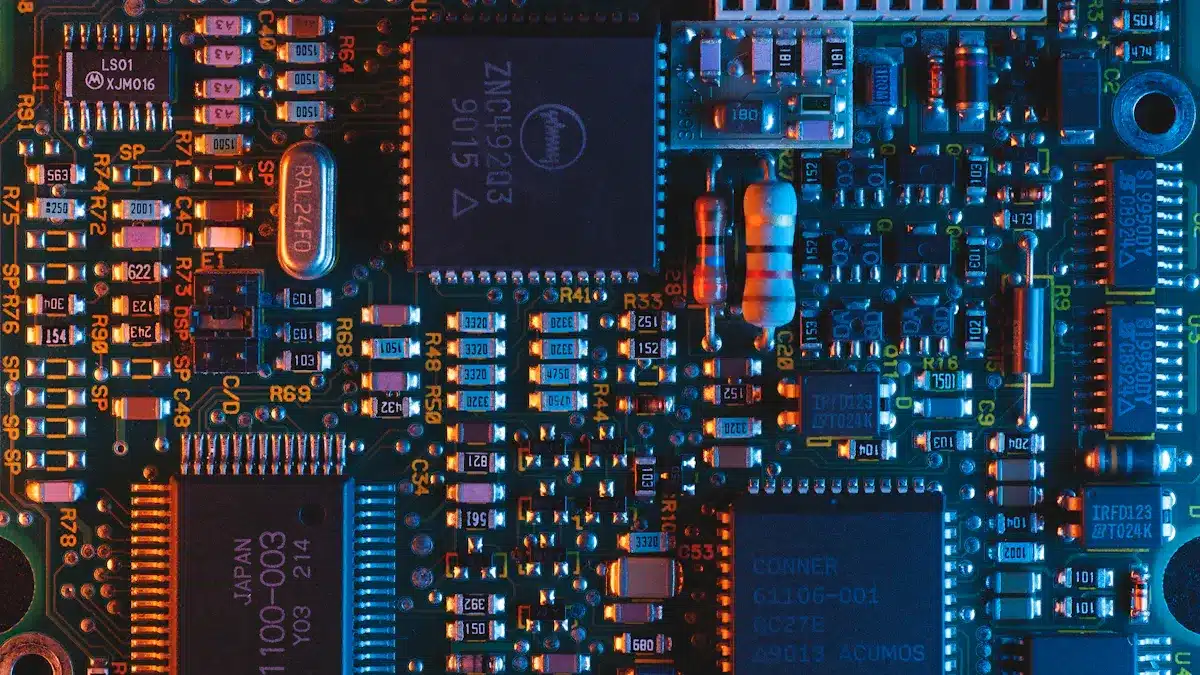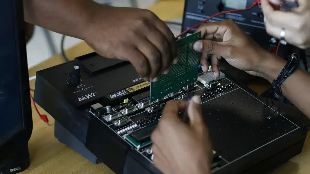
Printed circuit boards (PCBs) play a crucial role in electronics, serving as the main component in many devices such as smartphones and computers. Understanding the printed circuit board fabrication process gives you insight into the detailed work involved in creating these essential parts. This fabrication process includes several key steps:
Layer alignment
Drilling
Plating
Final assembly
Each step in the printed circuit board fabrication process ensures the creation of a durable and efficient PCB tailored to your electronic requirements.
Key Takeaways
The PCB making process has design, layer alignment, drilling, plating, and final assembly. These steps help create strong circuit boards.
Good designs for schematics and layouts lower mistakes. They also improve signal quality and cut down costs.
Copper patterning and etching create the electrical paths. They also affect how well the PCB manages current and heat.
Drilling makes holes that connect the layers. Using the right drilling method and via type helps the PCB work better and last longer.
Plating and solder mask protect the PCB. They also make sure the electrical connections are strong. Final quality checks find problems before shipping.
PCB Design Process
The PCB design process is an important step in making printed circuit boards. It sets up how the PCB will work in electronic devices. You need to focus on both schematic design and layout design for a good result.
Schematic Design
Schematic design is like a map for your PCB. It shows the electrical connections and where the parts go. A correct schematic helps reduce mistakes that can cause problems or expensive changes. Here are some benefits of a good schematic design:
It makes things clear and helps with documentation, which makes fixing problems easier.
Testing through simulation finds problems before making a physical model.
A good schematic helps with the PCB layout, where placing parts relies on its accuracy.
To make good schematics, you can use different software tools. Here is a table of some popular choices:
Software Tool | Key Features Relevant to Schematic Design and PCB Development |
|---|---|
Altium Designer | Easy to use, 3D view, teamwork features, lots of integrations, a top choice for experts. |
Allegro PCB Designer | Analyzes signal quality, advanced wiring, big library of parts, great for fast designs. |
Autodesk EAGLE | Large parts library, works with Autodesk Fusion 360, easy to use, good for small companies and beginners. |
KiCad EDA | Free and open-source, active community, works on many systems, checks design rules (DRC), good for students and beginners. |
Layout Design
After you finish the schematic, you start layout design. This step is about placing parts on the PCB and connecting the electrical paths. Good layout design is key for making and using the PCB well. Here are some best practices to keep in mind:
Use the same grid spacing and avoid using different grids to stop design problems.
Keep paths short and straight, and avoid sharp bends to improve signal quality.
Group similar parts together to make design and testing easier.
Regularly check design rules (DRC) to find mistakes early.
The layout design affects the cost and how easy it is to make printed circuit boards. For example, making the design simpler can lower costs and help with manufacturing. Also, thinking about manufacturability early can spot issues, leading to faster production and less waste.
When you change your design files into formats ready for manufacturing, like Gerber files, you make sure your PCB can be made correctly. PCB design software like Altium Designer or KiCad lets you save your design in these formats. This step is important to avoid mistakes and ensure the manufacturing files match your original design.
By knowing the PCB design process, you can create effective and reliable printed circuit boards that fit your electronic needs.
Inner Layer Steps

Making the inner layers of a printed circuit board (PCB) has several important steps. These steps help the PCB work well and meet the design needs.
Copper Patterning
Copper patterning is important for showing the paths that electricity will follow on your PCB. This process affects how well the board works. Here are some key points about copper patterning:
It decides how much current can flow, the voltage drop, and how heat is released.
Copper conducts electricity well, which helps signals travel with little power loss.
The thickness of copper patterns changes electrical resistance. Thicker copper layers lower resistance, allowing more current to flow.
Copper also helps get rid of heat from parts, stopping them from overheating.
Good soldering on copper makes sure connections between parts and PCB traces are strong.
To make the inner layers, you start by sticking copper foil onto an insulating core. Then, you use photolithography to put circuit patterns on the copper foil. After that, you use chemicals to remove extra copper and create the needed circuits. This careful process helps define power and ground planes, which improves signal quality and voltage stability.
Etching Process
The etching process is very important for taking away unwanted copper and showing the circuit patterns. You can use different methods for etching, each with its benefits:
Wet Etching: This method uses chemical solutions to dissolve copper. It is cheap and commonly used in PCB making. However, it needs careful control to avoid damage.
Dry Etching: This technique uses plasma or ion beams to remove copper without liquids. It is more precise and better for the environment but usually costs more.
Laser Etching: This method uses a focused laser beam to take away unwanted copper. It is accurate and does not touch the board, which reduces stress. However, it is not great for large boards because it costs more.
The etching process has several steps:
Get the substrate ready by choosing the right base materials and cutting them to size.
Stick photosensitive dry film onto the semi-cured sheets to prepare for image transfer.
Make inner layer circuits by transferring circuit patterns using photolithography.
Etch the inner layer to remove unwanted copper, leaving the needed circuit traces.
Check the inner layers with microscopes or X-ray to ensure quality and accuracy.
By learning the copper patterning and etching processes, you can create strong inner layers that help your printed circuit boards work better.
Drilling and Vias

The drilling process is very important in making PCBs. It makes holes that connect different layers of the board. These holes let electrical signals pass through. This helps the PCB work correctly. There are different drilling methods, and each has its benefits.
Drilling Techniques
Common drilling machines are vertical and horizontal ones. Vertical machines are good for single-sided and double-sided PCBs. Horizontal machines work better for multilayer boards. Mechanical drilling uses rotating bits made of tungsten carbide. This method is cheap and works for standard hole sizes. But, it may not be good for very small holes.
Laser drilling is another method. It makes tiny holes down to 0.002 inches (0.05 mm) with great accuracy. This method is best for high-density interconnect (HDI) PCBs, which are often in compact devices like smartphones. Laser drilling reduces mechanical stress, making it good for delicate designs.
Using accurate drilling methods improves the quality and yield of your PCBs. For example, teardrop shapes around vias help connections and lower defects. This design feature makes the PCB stronger and helps prevent misalignment.
Via Types
Vias are important for connecting different layers of a PCB. Here are the main types of vias you should know:
Through-Hole Vias: These go through the whole PCB, connecting all layers. They are simple and cost-effective.
Blind Vias: These connect an outer layer to one or more inner layers without going through the whole board. They save space and make things less complicated.
Buried Vias: These connect only internal layers and cannot be seen from the surface. They are useful for high-density multi-layer PCBs.
Microvias: These are very small vias used in HDI PCBs. They connect nearby layers, allowing for compact designs.
Vias help with electrical connections and save space in your PCB layout. They also improve electrical performance and help with thermal management. Knowing the drilling methods and types of vias will help you make effective and reliable printed circuit boards.
Plating and Coating
The plating and coating steps are very important in making PCBs. They help create electrical connections and protect the board from damage. There are two main types of plating: electroless and electroplating.
Electroless and Electroplating
Electroless copper plating is a chemical method. It adds a thin layer of copper to the non-conductive walls of drilled vias. This step makes a conductive seed layer. This layer is important because the drilled holes do not conduct electricity. After this seed layer is made, electroplating uses electric current to add more copper. This makes the vias and traces thicker, stronger, and better at conducting electricity. Together, these steps ensure strong electrical connections between PCB layers. They provide pathways through vias and a strong surface for soldering parts. This strength is key for keeping signals clear and the PCB strong.
Common materials used for plating include:
Copper: Great for electrical conductivity, it is used for through-hole and surface plating.
Silver: Has excellent conductivity and is best for high-speed uses.
ENIG (Electroless Nickel Immersion Gold): Resists corrosion and is great for soldering.
HASL (Hot Air Solder Leveling): A cheaper finish but not good for fine-pitch parts.
Solder Mask Application
The solder mask is a protective layer on the PCB. It has several important jobs:
It acts as an electrical insulator, stopping unwanted electrical contact and short circuits.
It protects metal tracks from moisture, dust, and chemicals.
It helps prevent corrosion and oxidation, making it more reliable.
It helps place components correctly during assembly, reducing mistakes.
You can apply solder masks in different ways. The Liquid Photoimageable (LPI) solder mask is the most common. This method uses a liquid mixture that hardens when exposed to UV light. Other methods include epoxy screen printing and dry film solder masks, each with its own benefits.
By learning about the plating and coating steps, you can see how they help make printed circuit boards strong and effective.
Final Steps in PCB Fabrication
The last steps in the printed circuit board fabrication process are very important. They make sure your PCBs meet the right standards and quality. These steps include profiling and cutting, along with careful quality checks.
Profiling and Cutting
Profiling is the final step where you cut the PCBs from the main panel. This process shapes each PCB to the right size using design files. Here are the common ways to profile:
Routing (Scoring): This method makes small tabs on the edges. It helps separate the boards easily after cutting.
V-Cut: This technique makes V-shaped grooves. It lets you snap the boards apart neatly.
Hard Tooled Punches: In large production, manufacturers may use these for fast cutting.
After profiling, you do a final visual check and quality inspection. This makes sure the PCBs are free of errors before they are packaged and shipped. Here’s a summary of the profiling process:
Identify the shape and size of each PCB from the main panel.
Use routing or V-cutting to create the right outline.
Conduct a thorough inspection to check hole positions, board sizes, and cleanliness.
The quality of the edges matters too. Different profiling methods can affect edge quality. For example, laser cutting gives the best precision with clean edges, while punching may lead to lower quality with possible micro-cracks. Here’s a comparison of profiling methods:
Profiling Method | Edge Quality | Key Characteristics | Suitable Applications |
|---|---|---|---|
Laser Cutting | Highest precision; clean, smooth edges with minimal burrs | Non-contact process; tight tolerances; higher cost | High-end PCBs needing tight accuracy |
Punching | Lower edge quality; possible micro-cracks | Very fast; needs hard tools; lower accuracy | High-volume production where speed is key |
Routing | Good edge quality; smooth edges | Versatile; tolerances ±0.003-0.005 in | Small to medium batch sizes; prototyping |
V-Cut | Relatively poor edge quality; jagged edges | Fast and low cost; limited to straight lines | Simple shapes; high-volume production |
Quality Assurance
Quality assurance is very important in the last stages of making PCBs. It ensures that every board meets strict standards before reaching customers. Various tests check the strength and function of the PCBs. Here are some common quality assurance tests:
Solder Float Testing: Checks thermal stability by exposing the PCB to hot solder.
Peel Test: Measures how strong the copper traces stick.
Flying Probe Testing: Tests electrical connections using movable probes.
Visual Inspections: Automated Optical Inspection (AOI) finds solder defects and checks component placement.
These tests help find problems that could cause failures later. Common causes of failure found during this stage include:
Manufacturing issues like misaligned layers.
Soldering problems causing electrical breaks.
Environmental stresses like heat and moisture.
By using strict quality control, manufacturers can lower defect rates. The average defect rate for PCBs after final quality checks is usually between 0.08% and 0.97%. This shows how effective quality assurance is in making reliable and strong PCBs.
Knowing how the printed circuit board (PCB) fabrication process works is important for anyone in electronics. Each step, from design to quality checks, is key to making sure the final product is reliable and works well. For example, drilling and plating create exact electrical connections that are necessary for the device to function. Solder masks protect the board from damage, making it last longer.
By understanding these steps, you can make better design choices, save money, and boost device performance. This knowledge also helps you talk clearly with manufacturers and keep up with new technology. In the end, knowing the PCB fabrication process leads to high-quality electronic devices that fit your needs.
FAQ
What is a printed circuit board (PCB)?
A printed circuit board (PCB) is a flat board that connects electronic parts. It has pathways that let electricity flow between the parts. This helps devices like smartphones and computers work.
How long does the PCB fabrication process take?
The PCB fabrication process usually takes one to four weeks. Things like how complex the design is, its size, and how busy the manufacturer is can change the time. Always ask your manufacturer for exact lead times.
What materials are used in PCB fabrication?
Common materials for PCBs are fiberglass, epoxy resin, and copper. These materials are strong and help electricity flow well, making sure the PCB works properly in electronic devices.
Can I design my own PCB?
Yes, you can design your own PCB with different software tools. Programs like Altium Designer and KiCad let you create schematics and layouts that fit your needs.
How do I ensure the quality of my PCB?
To make sure your PCB is good quality, test it carefully during fabrication. Use methods like visual checks, solder float testing, and flying probe testing. These tests help find problems and ensure it works reliably.
See Also
Key Stages Involved In The PCBA Production Process
Detailed Walkthrough Of The PCBA Manufacturing Procedure
Understanding SMT Techniques Within PCBA Assembly Workflow