PCB stands for Printed Circuit Board in electronics. So, what does PCB stand for? It is a flat board that does not conduct electricity, with copper lines on it. These copper lines connect electronic parts together, enabling devices to function properly. PCBs are found in phones, watches, and smart home gadgets—products that play an important role in your daily life. The PCB market was valued at $67.9 billion in 2023 and is growing rapidly.
Here’s a quick look at how PCB use has changed in consumer electronics:
Aspect | Evidence Supporting Increased PCB Adoption in Consumer Electronics |
|---|---|
Market Size & Growth | The global PCB market was $67.9 billion in 2023. It may reach $92.4 billion by 2029. The growth rate is 5.4% each year. |
Demand Drivers | More people want electronics and IoT devices. This includes phones, watches, and smart home gadgets. |
Technological Advances | New types of PCBs help make small and powerful devices. These include multilayer and HDI PCBs. |
Key Takeaways
PCB means Printed Circuit Board. It is a flat board. It connects electronic parts with copper lines. These lines help devices work.
There are three main PCB types. Single-sided PCBs are for simple devices. Double-sided PCBs hold more parts. Multilayer PCBs are for complex electronics like smartphones.
PCBs use materials like FR-4 fiberglass. This makes them strong and safe. Copper traces carry electricity between parts.
PCBs give electrical connections and mechanical support. They keep parts linked and secure inside devices.
PCBs are important in everyday electronics. They help devices get smaller, faster, and more reliable.
What Does PCB Stand For
PCB Meaning
If you ask, “what does pcb stand for,” you find out it means Printed Circuit Board. You see this word in many electronics books and guides. It is also in product manuals and school science projects. Big electronics groups like IPC, UL, ISO, and IEC all have rules for printed circuit boards. IPC tells you how to design and build a PCB. UL checks if the materials are safe. ISO makes sure the boards are made well. IEC sets rules for quality around the world.
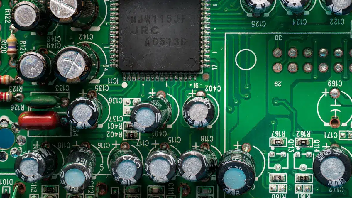
A printed circuit board is a flat plate that does not let electricity pass through. Copper lines are printed or etched on this plate. These copper lines join electronic parts, like resistors and chips. When you look inside a device, you often see a green board with shiny paths. That is the PCB. Sometimes people say PWB, which means Printed Wiring Board. Some use PWB and PCB for the same thing, but PCB is used more.
PCBs are in almost every electronic device. The board holds the parts and lets electricity move between them. There are single-sided, double-sided, and multilayer PCBs. Each type is used for different things. A single-sided PCB is good for simple toys. A multilayer PCB is used in smartphones or computers.
Tip: If you open a remote control or game console, look for a green or blue board with copper lines. That is the PCB. It helps your device work.
PCB in Electronics
You may wonder, “what does pcb stand for” in electronics. The answer is easy. PCB means Printed Circuit Board. It is the main part of most electronic devices. You use a PCB to hold and connect many parts, like chips, capacitors, and connectors. The copper lines carry signals and power to each part.
Printed circuit boards come in many shapes and sizes. Big PCBs are inside desktop computers. Small ones are inside smartwatches. The board is usually made from fiberglass or epoxy. This keeps it strong and safe. Copper is used for the lines. It helps electricity move fast.
You might see PWB in old books or papers. PWB means Printed Wiring Board. It is another name for PCB. Today, most people say PCB.
Here is a table to help you see the difference between a PCB and other circuit carriers:
Feature | Printed Circuit Board (PCB) | Integrated Circuit (IC) |
|---|---|---|
Function | Gives support and connects parts | Does special jobs like logic and control |
Material | Made from fiberglass, epoxy, copper | Made from silicon |
Size | Bigger, changes by use | Very small, just a few millimeters |
Components Hosted | Holds many parts like ICs, resistors, capacitors | Has tiny parts inside like transistors |
Complexity | Can be simple or have many layers | Very complex even though it is small |
Location in System | Main platform for parts | Put on the PCB as a part |
Role Together | PCB gives support; IC does thinking and control | ICs need PCB to work and connect |
A PCB gives shape and connections. An IC does the thinking and controlling. You need both to make a device work.
When you ask, “what does pcb stand for,” you learn it means more than just a board. It is a key part of every electronic device you use. Printed circuit boards help you use technology every day, like your phone or TV.
Printed Circuit Board Structure
Layers and Materials
When you look at a printed circuit board, you see a strong, flat plate. This plate is made from layers of different materials. There are copper layers that let electricity move. There are also layers that keep things safe and hold the board together. The most common material for these layers is called FR-4. FR-4 is a type of fiberglass mixed with epoxy. It does not burn easily and makes the board strong. Some boards use other materials like ceramics, polyimide, or metal-core for special jobs.
Here is a table that shows the main materials used in printed circuit boards and their properties:
Material | Properties | Typical Applications |
|---|---|---|
FR-4 | Strong, flame-retardant, low water absorption, cost-effective | General purpose PCBs, multi-layer boards, prototyping |
Rogers | Low dielectric constant, stable at high frequencies | RF power amplifiers, antennas |
Polyimide | Flexible, heat resistant, good electrical properties | Flexible PCBs, wearables, aerospace |
PTFE (Teflon) | High temperature stability, chemically inert | High-frequency circuits, aerospace |
Ceramic | High thermal conductivity, high operating temperature | High-power LEDs, medical devices |
CEM Series | Lower cost, varying mechanical and dielectric properties | Consumer electronics, single and double-sided PCBs |
LCP | Low moisture absorption, stable over wide temperature range | 5G antennas, flexible modules |
Metal-Core PCBs | Metal base for heat dissipation | LED lighting, motor drives |
Each material helps the board work in its own way. FR-4 is used the most because it is cheap and strong. Polyimide is good for boards that need to bend. Ceramics are picked when the board must handle a lot of heat.
The number of layers in a printed circuit board changes how it works. Simple devices use single-layer boards. Double-layer boards give more room for parts and better signals. Multi-layer boards are used in things like computers and smartphones.
Performance Impact | Typical Applications | |
|---|---|---|
Single-layer | Simple, cost-effective; limited circuit density | Basic electronics, toys, household appliances |
Double-layer | More parts, better signals, improved power distribution | Computer motherboards, medical devices |
Multi-layer (3+) | High density, better signal quality, compact size | Smartphones, advanced electronics |
Tip: When you design a pcb layout, you pick the number of layers and materials based on what your device needs.
Copper Traces and Substrate
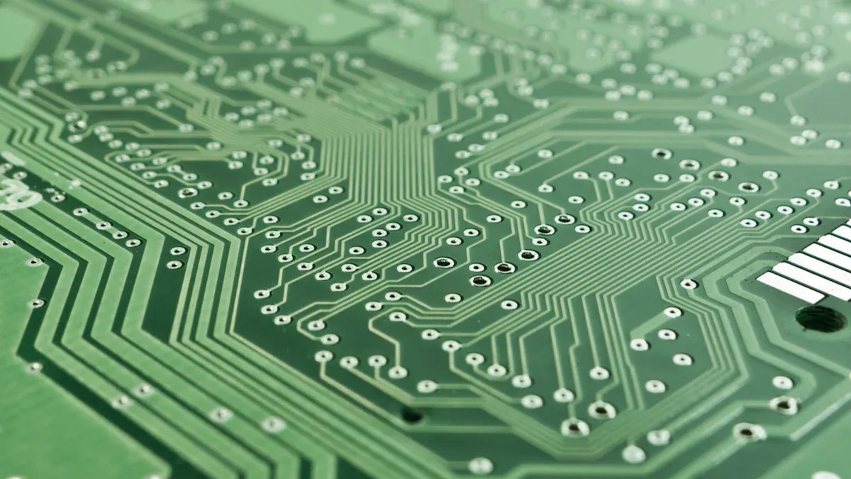
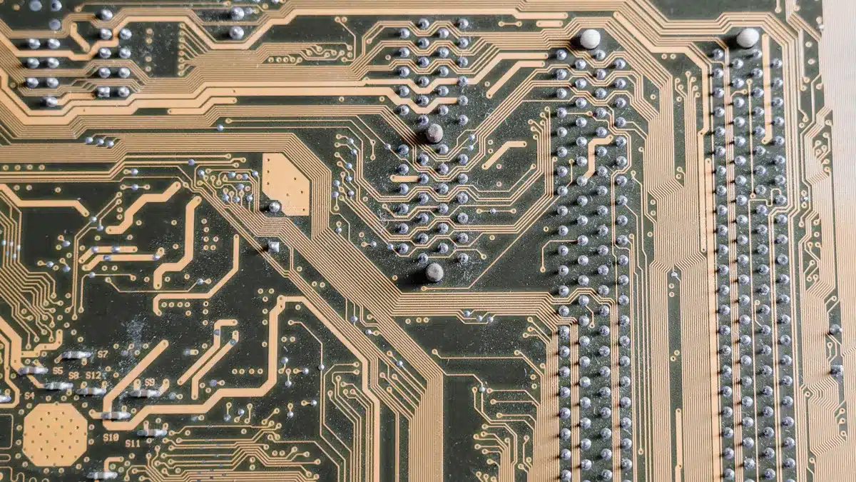
Every printed circuit board has copper traces. These thin lines move electricity between parts. Most boards use copper that is 1 oz per square foot thick. This is about 0.035 mm. This thickness is strong and lets enough electricity flow. If you need more power, you can use thicker copper.
The substrate is the bottom layer of the board. FR-4 is the most common substrate. To make it, workers start with fiberglass sheets and cover them with epoxy. They add copper foil on top. Then, they use light and chemicals to make the circuit pattern. Machines drill holes for the parts and connections. After that, they cover the holes with copper and put on a solder mask for protection. The last step is testing the board to make sure it works.
Here is a simple list of how manufacturers build an FR-4 substrate for a printed circuit board:
Get fiberglass sheets and cover them with epoxy.
Put copper foil on the surface.
Use photoresist and UV light to make the circuit pattern.
Remove extra copper to make the traces.
Drill holes for parts and connections.
Cover the holes with copper for paths.
Add solder mask and silkscreen for protection and labels.
Test and cut the board to the right size.
When you plan a pcb layout, you must think about copper thickness, trace width, and the type of substrate. These choices change how well your board works and how long it lasts.
Circuit Board Types
When you look at electronics, you see different circuit boards. Not every board looks or works the same way. There are three main types of circuit boards. These are single-sided, double-sided, and multilayer. Each type is used for different devices and jobs.
Single-Sided
A single-sided circuit board has copper lines on one side only. All the parts and wires are on the same surface. Most single-sided boards use FR-4 or CEM-1 materials. The copper layer is covered to keep it safe. These boards are best for simple circuits with few parts. You find them in toys, small lights, and easy control panels.
Single-sided boards have a simple design.
All the parts go on one side, so building is easy.
These boards cost less, which saves money.
You cannot add many parts because of the design.
Feature | Single-Sided PCBs |
|---|---|
Construction | |
Cost | Cheap to make |
Applications | Used for simple circuits |
Design Complexity | Easy to plan |
Manufacturing | Fast and simple |
Tip: If you open a remote or night light, you may see a single-sided board.
Double-Sided
A double-sided circuit board has copper on both sides. You can put parts and lines on the top and bottom. This lets you fit more things in a small space. Vias connect the two sides, so signals can move between layers. Double-sided boards are good for harder circuits than single-sided ones.
You can use both through-hole and surface mount parts.
These boards hold more parts in less space.
Making these boards takes more time and skill.
Double-sided boards are found in phones, amplifiers, and car dashboards. They are used when you need small size and more features.
Multilayer
A multilayer circuit board has three or more copper layers. Each layer is separated by an insulating material. You use this board for high performance and lots of connections. Multilayer boards are in smartphones, computers, and medical machines.
These boards have special ground and power layers for better signals.
They help cut down noise and keep signals clear.
You can make very hard circuits with lots of parts.
The board stays small, even with many features.
Multilayer boards are used in many areas:
Medical: X-ray machines, heart monitors
Automotive: electric cars, sensors
Aerospace: avionics, radar
Note: Multilayer boards help fast electronics work better by lowering noise and keeping signals strong.
PCB Importance
Electrical Connection
You use a pcb every time you turn on a device. One big job of a pcb is to link all the parts together. The copper traces work like tiny roads. These roads move signals and power from part to part. This neat setup helps your device run well and keeps signals strong.
A pcb gives you many good things for electrical links:
It gives a steady place to put all the parts.
The pcb design lowers the chance of short circuits.
Careful planning stops noise and signal loss.
A pcba is a pcb with all the parts already put on. This makes sure every link is tight and works well. You do not have to worry about loose wires or messy setups. The layers in a pcb, like the base and solder mask, keep the links safe and hold everything in place.
Tip: Smart pcb design helps your device work better and last longer.
Mechanical Support
Another big job of a pcb is to hold all the parts in place. The pcb keeps each part where it should be, even if you drop or shake your device. This keeps things lined up and working right.
Here is a table that shows how different pcb types handle stress:
PCB Type | Mechanical Strength | Best Use Cases |
|---|---|---|
Hard, does not bend | Computers, cars, appliances | |
Flexible pcb | Bends, takes in stress | Wearables, phones, cameras |
A pcba uses these strengths to help your device last. The pcb acts like a backbone, holding parts during bumps and heat changes. Flexible pcbs can bend and fit into tight spots, making gadgets smaller and lighter. This is possible because the pcb lets you put many parts close together and still stay strong.
You can count on a pcba to keep your device working, even when things get rough. The pcb works as both the electric road and the strong frame for your electronics.
PCB in Devices
Everyday Electronics
You use a pcb every day, even if you do not see it. Your smartphone, laptop, and smartwatch all depend on a pcb or a pcba to work. In a smartphone, you find different types of pcb. Multilayer pcb supports the complex circuits inside. Flexible pcb fits into tight spaces and lets your phone bend a little without breaking. Rigid-flex pcb combines both types, making your device strong and flexible at the same time.
PCB Type | Characteristics | Common Applications in Smartphones and Laptops |
|---|---|---|
Multilayer PCB | Multiple copper layers for complex circuits | Laptops, smartphones |
Flexible PCB | Thin, bendable, fits small spaces | Smartphones, wearables |
Rigid-Flex PCB | Mix of rigid and flexible sections | Smartphones, cameras, laptops |
Wearable devices like fitness trackers and smartwatches use a special kind of pcb. Flexible and rigid-flex pcb let these devices bend and move with your body. You get comfort and accuracy because the pcba can fit into small, curved spaces. These pcb also help keep your device light and thin. In medical wearables, ultra-thin flexible pcb make sure the device feels comfortable and works safely.
You rely on a pcba to connect sensors, batteries, and screens in one small package. The pcba keeps signals clear and strong, even when you move. It also helps your device send data to your phone or the cloud using Bluetooth or Wi-Fi.
Tip: Next time you check your smartwatch or fitness band, remember that a flexible pcb inside helps it track your steps and heart rate.
Manufacturing Basics
You might wonder how a pcb or pcba is made. The process starts with picking the right materials, like FR-4 fiberglass or polyimide. Workers print the circuit pattern onto the board using a special film. They use chemicals to remove extra copper, leaving only the needed traces. Machines drill tiny holes for parts and connections.
After drilling, the pcb gets a copper coating and a solder mask for protection. The surface finish, like HASL or ENIG, helps parts stick better. In the assembly step, workers or robots place chips, resistors, and other parts onto the pcb. This turns the pcb into a pcba.
Here are the main steps in making a pcb and pcba:
Select the right material for the job.
Print the circuit pattern on the board.
Etch away extra copper.
Drill holes for parts and vias.
Plate the holes and add a solder mask.
Apply a surface finish to the pads.
Mount parts using THT or SMT.
Test the pcba for errors.
Check quality with machines and by hand.
Pack and ship the finished pcba.
Quality control is very important. Automated Optical Inspection (AOI) checks for missing or misplaced parts. X-ray inspection looks for hidden problems. In-circuit testing and functional tests make sure the pcba works as it should. These steps help you get a safe and reliable device.
Note: Every pcba in your electronics goes through many tests before it reaches you. This keeps your devices working longer and safer.
You now know that a pcb is the backbone of modern electronics. It connects and supports every part inside your favorite devices. The global pcb market keeps growing, driven by new technology and high demand for smart products.
PCBs help make devices smaller, faster, and more reliable.
You see pcbs in phones, cars, and even medical tools. As technology advances, you will find even more uses for pcbs in your daily life.
Year | Global PCB Market Size |
|---|---|
2023 | |
2029 (est) | $92.4 Billion |
FAQ
What is the main job of a PCB?
A PCB connects and supports electronic parts. You use it to link chips, resistors, and sensors. Copper traces carry signals and power so your device works smoothly.
Can you recycle old PCBs?
You can recycle old PCBs. Special companies remove metals like copper and gold. Recycling helps protect the environment and saves resources.
Why do most PCBs look green?
Most PCBs look green because manufacturers use a green solder mask. This layer protects copper traces and makes the board easier to inspect.
How do you spot a PCB inside a device?
You find a PCB by looking for a flat board with shiny copper lines. It often has a green or blue color. You see small parts attached to it.
What happens if a PCB breaks?
If a PCB breaks, your device may stop working. You might see errors or lose power. You need to replace the PCB or repair it to fix the problem.
See Also
Understanding PCBA And Its Definition In Electronics
The Importance Of PCB Design In Modern Electronics
Exploring The Meaning And Function Of PCBA In Electronics
Defining PCBA And Its Significance Within Electronics
Breaking Down PCBA Abbreviation And Its Electronic Relevance