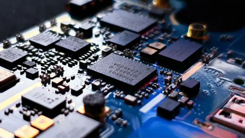

In today’s world, technology is very important in your daily life. Most electronic devices have a printed circuit board (PCB) inside, which is the pcb full form in electrical. This key part connects different electronic pieces, helping them work together smoothly. The worldwide market for PCBs is growing fast and is expected to reach $73.1 billion by 2024. Learning what PCB means in electrical is just the start; it helps you see how these boards affect modern technology and new ideas.
Key Takeaways
Printed Circuit Boards (PCBs) are important for connecting electronic parts. They are key in devices like smartphones and computers.
PCBs have different types: single-sided, double-sided, and multi-layer. Each type is good for certain uses and levels of complexity.
PCBs help devices work better. They improve signal quality, allow more parts, and make designs smaller.
Knowing how to design and make PCBs helps create reliable and efficient electronic devices.
As technology grows, PCBs will keep being important for new ideas in many fields, like healthcare and cars.
What is a Printed Circuit Board?
A printed circuit board (PCB) is an important part of modern electronics. It acts as a base that holds and connects the parts of an electric circuit. This connection is the base for almost all electronic devices you see every day. The pcb full form in electrical shows how it helps make electrical connections through special paths.
PCB Full Form in Electrical
The short form “PCB” means Printed Circuit Board. This name describes a flat board made from materials that do not conduct electricity, like fiberglass. On this board, paths are made to connect different electronic parts. These connections help devices work properly and efficiently.
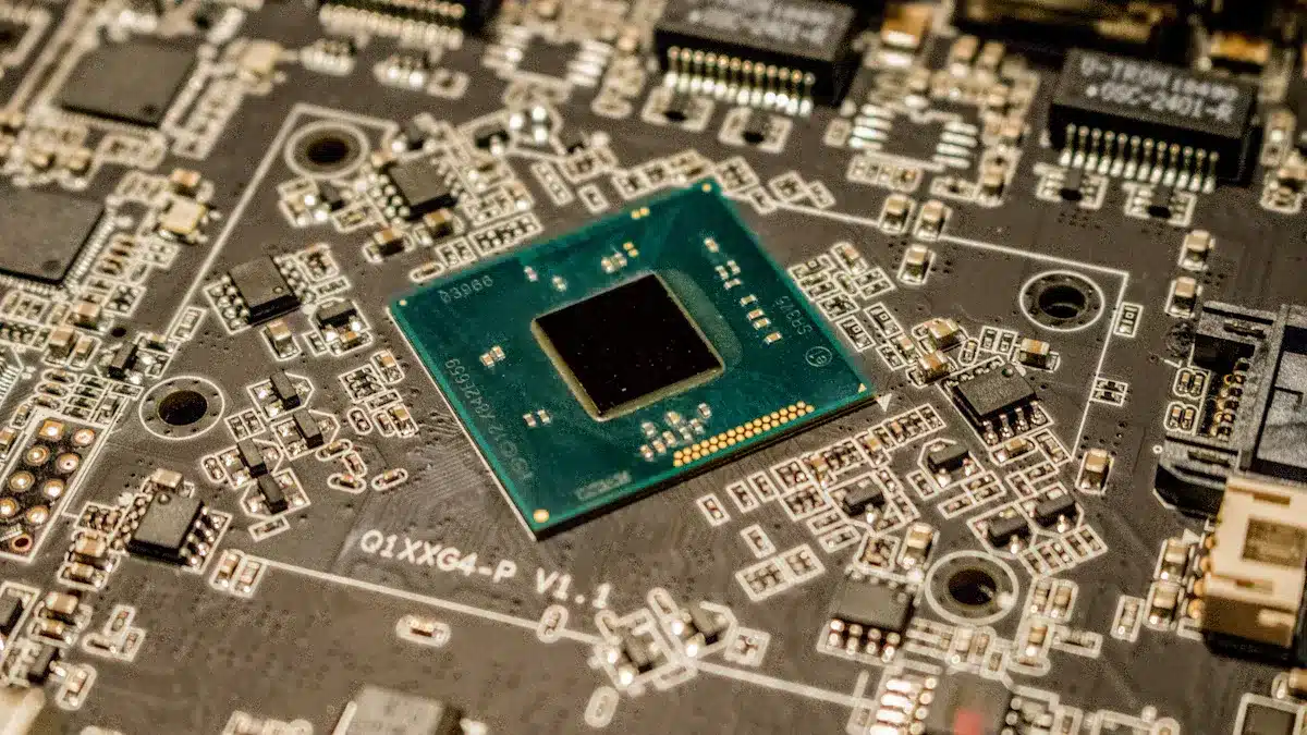
Components of a PCB
Knowing the parts of a PCB helps you see why it is important. Here are the main parts found on a standard printed circuit board:
Passive components: These are resistors, capacitors, and inductors. They help with signals, filtering, and controlling voltage.
Active components: Integrated circuits (ICs), transistors, and diodes manage current flow and do different tasks.
Connectors and interfaces: Headers and ports, like USB or HDMI, let you connect to other devices.
Power management components: Voltage regulators keep voltage levels steady for proper operation.
The structure of a PCB usually has several layers. Here’s a look at its typical structure:
Substrate layers: The base material, often fiberglass (FR4), gives strength and insulation.
Copper traces: These paths carry electrical signals between different parts.
Solder mask: This layer protects and insulates the copper traces from damage and short circuits.
Silkscreen: Labels and symbols printed on the board help with placing and identifying parts.
PCBs have many layers of copper and insulating materials. This design makes electrical connections while supporting electronic parts. The table below shows the main functions of a printed circuit board in electronic devices:
Function | Description |
|---|---|
Mechanical Support | Gives a strong platform for parts, keeping them in place and safe from stress. |
Electrical Connectivity | Makes paths for signals and power, allowing complex routing in small spaces. |
Thermal Management | Moves heat away from parts and includes cooling methods to avoid damage. |
Signal Integrity Preservation | Keeps signal quality high through controlled impedance and protection from interference. |
Miniaturization Enablement | Supports small designs using advanced connection methods and flexible PCB options. |
Types of Printed Circuit Boards
Printed circuit boards (PCBs) come in different types. Each type is made for specific uses and levels of complexity. Knowing these types helps you pick the right PCB for your project.
Single-Sided PCBs
Single-sided PCBs have one layer of conductive material on one side. All components are placed on this same side. This design is simple and cheap, making it great for basic electronic circuits. Common uses include:
Consumer electronics like calculators and LED displays
Simple medical devices and toys
Remote controls and basic IoT products
Single-sided PCBs are best for low-density uses where there are few components.
Double-Sided PCBs
Double-sided PCBs have conductive material on both sides. This lets you place components on either side, which increases the circuit density. You can connect both sides using plated through holes (PTH). This design works for more complex circuits and is good for uses like:
Industrial controls and automotive electronics
Audio and RF amplifiers
Double-sided PCBs have benefits like higher component density and better electrical performance. However, they are also more complex to design and make. Here’s a quick look at their pros and cons:
Advantages of Double-Sided PCBs | Disadvantages of Double-Sided PCBs |
|---|---|
Higher component density | Increased fabrication complexity |
Better electrical performance | Longer design and assembly times |
Improved signal integrity | More challenging troubleshooting |
Multi-Layer PCBs
Multi-layer PCBs have many layers of conductive material with insulating layers in between. This design allows for high circuit density and better signal quality. You often see multi-layer PCBs in advanced uses like:
Computer motherboards and telecommunications equipment
Medical devices and military applications
These PCBs help manage heat and reduce electromagnetic interference. They are great for compact and high-performance electronics.
Structure Description | Applications | |
|---|---|---|
Single Sided PCBs | One layer of conductive material on one side, components mounted on the same side. | Consumer electronics, LED lighting, basic power supplies. |
Double Sided PCBs | Conductive material on both sides, components can be mounted on either side. | Industrial controls, automotive electronics, audio and RF amplifiers. |
Multi-layer PCBs | Multiple layers of conductive material separated by insulating layers. | Computer motherboards, telecommunications equipment, medical devices. |
Knowing these types of PCBs helps you make smart choices when designing or picking parts for your electronic projects.
Applications of Printed Circuit Boards
Printed circuit boards (PCBs) are very important in many industries. They are reliable and flexible, making them key parts in many uses. Let’s look at how PCBs are used in consumer electronics, cars, and medical devices.
Consumer Electronics
You find printed circuit boards in almost every electronic device you use every day. These boards help many products work properly. Some common uses include:
Smartphones
Tablets
Smartwatches
Radios
Computers
Televisions
Stereos
Video game consoles
Home appliances (like refrigerators, microwaves, coffee makers)
As technology improves, the need for smaller and better PCBs grows. Companies work hard to fit many functions into small designs. This trend leads to new consumer electronics that make your life better.
Automotive Industry
The automotive industry depends a lot on printed circuit boards. Modern cars use many electronic parts, so PCBs are crucial for many systems. Here are some key uses of PCBs in cars:
Airbag systems
Audio and video systems
Global positioning systems (GPS)
Anti-lock brakes
Communication tools
Engine timing systems
LED brake lights
Remote diagnostics
Security systems
Transmission sensors
Printed circuit boards help make modern cars safer. Safety PCBs in cars work in many ways. For example, they control airbag systems, advanced driver-assistance systems (ADAS), and anti-lock braking systems (ABS). These uses help cars run safely and well.
Medical Devices
In medicine, printed circuit boards are key for many devices. They make complex circuits easier and ensure they work well. Here are some ways PCBs help in medical technology:
PCBs make complex circuits easier and ensure they work well in medical devices.
Their small size and high performance make them great for portable medical devices.
They use advanced technologies like IoT and AI for real-time health checks.
PCBs provide important connections and functions for many medical uses. They ensure reliability, accuracy, and the use of advanced technologies in healthcare. You can find them in devices like x-rays, infusion pumps, and blood glucose monitors. Also, PCBs help with remote monitoring and telemedicine, which are more important in today’s healthcare world.
By learning about the uses of printed circuit boards, you can see how important they are in shaping modern technology in many industries.
PCB Importance in Electrical Engineering
Printed circuit boards (PCBs) are very important in electrical engineering. They are reliable and help electronic systems work well. You can trust PCBs to do their jobs over time. Many things make them reliable:
Design quality
Material properties
Manufacturing processes
Environmental conditions
Usage patterns
To make them more reliable, you should do thermal analysis when designing. This helps find hot spots. Using thermal vias and copper pours can help with heat flow. Also, adding heat sinks or fans for powerful parts can help them work better.
Reliability and Performance
The performance of advanced PCBs brings many benefits. Here are some key improvements from using them:
Increased Component Density: Advanced PCBs allow for fine lines and microvias, which means more parts can fit. This makes devices smaller.
Enhanced Signal Integrity: The design of advanced PCBs improves signal quality, which is important for high-performance electronics.
Miniaturization: These boards help create smaller, lighter devices without losing performance.
Improved Electrical Performance: Advanced PCBs boost electrical performance, making them good for tough jobs like quantum computing and aerospace.
Applications in Various Fields: They are used in IoT devices, advanced sensors, smartphones, car electronics, and medical devices, showing their importance in modern technology.
Innovation and Development
The growth of PCBs has led to big changes in electrical engineering. Their light and energy-saving design allows for complex tasks in many areas, like space exploration and consumer electronics. The design process of PCBs involves many people, which affects innovation in electrical systems. This process includes researching parts, making schematics, laying out the board, and checking everything, all of which help make electronic devices work better.
Recent tech advances in PCB design include:
Advancement Type | Description |
|---|---|
Lets smaller parts fit on PCBs, increasing density and making devices portable. | |
Flexible PCBs | Made from bendable materials, allowing twisting and turning, used in many applications. |
Improvements in Design Software | Makes it easier to create complex designs, leading to better electronic devices. |
3D Printing | Allows for new designs and less waste, helping with customization and faster manufacturing. |
By learning about the importance of PCBs in electrical engineering, you can see how they help with reliability, performance, and innovation in modern electronic devices.
Design and Manufacturing of PCBs
Designing and making printed circuit boards (PCBs) includes many important steps. Knowing these steps helps you understand how PCBs are created and how they work in electronic devices.
PCB Design Process
The PCB design process has several main steps. Each step is important to make sure the final product meets your needs. Here’s a simple list of the main steps:
Requirement analysis and Component selection: First, you define what the project needs and choose the parts.
In-System Front end design: Next, you create the first design layout and drawings.
Photo tool Initiation: You get the tools ready for the photolithography process.
Printing the inner layers: This step prints the inner layers of the PCB.
Etching out the unwanted copper: You take away extra copper to make the right circuit patterns.
Register punching for layer alignment: This makes sure all layers line up correctly when put together.
Automated optical inspection: You look for problems using automated systems.
Layer up and Bond: This step stacks and sticks the layers together.
Drilling: Finally, you drill holes for mounting parts and making electrical connections.
To help you with the design, there are many software tools available. Some popular PCB design software includes:
Altium Designer
Siemens PADS
Cadence Allegro
Eagle (Autodesk)
ORCAD
KiCAD
Fritzing
Upverter
EasyEDA
Proteus
These tools make the design process easier, helping you create complex circuit board designs.
Manufacturing Techniques
After finishing the PCB design, the next step is making it. There are several common methods used in PCB manufacturing. Here are some of the most popular techniques:
Etching: This old method removes unwanted copper to create circuit patterns.
Milling: CNC machines cut out the needed circuitry from a copper-covered material.
Additive Manufacturing: This method adds metal onto a base, allowing for high-density connections.
Drilling: This is important for making holes for mounting parts and electrical connections, using either mechanical or laser drills.
Through-Hole Plating: This process puts a conductive coating inside drilled holes to help parts stick properly.
Quality control is very important during PCB manufacturing. Different testing methods make sure the boards meet industry standards. Here’s a summary of some common quality control measures:
Testing Method | Description |
|---|---|
In-Circuit Testing (ICT) | Tests for open/short circuits and checks performance of integrated circuits using capacitance tests. |
Flying Probe Test | Finds loose connections and other problems without power using a probe aligned to a CAD grid. |
Functional Test | Makes sure the PCB works under test equipment while meeting industry standards. |
Automated Optical Inspection (AOI) | Finds missing parts and soldering problems using a camera system. |
X-Ray Inspection | Looks at internal structures of PCBs for shorts and openings not seen by the naked eye. |
Electrical Testing | Checks output signals against performance needs when the testboard is powered. |
Visual Inspection | Manual checks for physical damage like scratches and misalignment. |
By learning about the design and manufacturing steps of PCBs, you can see how these important parts come together to power modern electronics.
Printed circuit boards (PCBs) are very important in today’s electronics. They help make strong connections and allow for smaller designs. You can find PCBs in many fields, like healthcare, cars, and everyday electronics. Here are some important points to remember:
PCBs help with complex functions.
They improve how long devices last and how well they work.
Their growth keeps changing technology, leading to new ideas like flexible and 3D-printed PCBs.
As technology grows, PCBs will still be key in making new electronic devices. For more information, you can look into topics like PCB basics, soldering methods, and design software guides. 📚
FAQ
What materials are used to make PCBs?
PCBs usually use materials like fiberglass for the base, copper for the paths, and a solder mask for protection. These materials help make them strong and ensure good electrical connections.
How do I choose the right PCB type?
Think about how complex your project is and how much space you need. For simple circuits, use single-sided PCBs. If you have more parts, choose double-sided or multi-layer PCBs to save space and improve performance.
Can I design my own PCB?
Yes, you can design your own PCB with different software tools. Programs like Altium Designer and KiCAD let you create custom layouts that fit your needs.
What is the lifespan of a PCB?
The lifespan of a PCB depends on how you use it and the environment. Usually, a well-made PCB can last for several years, often more than 10 years in stable conditions.
How do I troubleshoot a faulty PCB?
To troubleshoot, first look for damage or loose connections. Use a multimeter to check for continuity and test each part one by one. This helps find the faulty areas easily.
See Also
Understanding PCB Design And Its Significance In Electronics
Defining PCBA In Electronics And Its Importance Explained
Exploring The Meaning Of PCBA And Its Function In Electronics
PCBA Explained: Its Meaning And Role In Electronics
Understanding PCBA Services And Their Importance In Electronics Production