
What is PCB assembly? It is a key process. It turns a bare PCB into a working electronic part. This process adds parts. These parts make the product work right. PCBs have been important since the 1950s. They are in almost all new electronics. About 70% of all PCBs go into things like phones, computers, and communication devices. This important process is growing fast. The market for PCB assembly will grow. It will grow 6.5% each year. This will happen from 2025 to 2032. This guide tells you all about this process. It covers the main steps. It also looks at what might happen in 2025. Knowing this process is key. It helps with making electronics. It helps with buying parts too.
Key Takeaways
PCB assembly turns a bare board into a working electronic device. It adds parts to make the product work right.
New PCB types like flexible and 3D boards are changing electronics. They need special ways to put them together.
The assembly process has many steps. These include design, part buying, solder paste, part placement, and soldering.
Quality checks and testing are very important. They find mistakes early and make sure the PCB works well.
Choosing the right partner for PCB assembly is key. They help make good products and meet quality standards.
Understanding the Bare PCB
What is a Printed Circuit Board
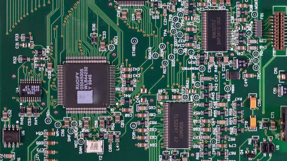
A Printed Circuit Board, or PCB, is a basic part. It is used in almost all electronics. It is a flat board. It is usually green. It holds and connects electronic parts. A bare PCB has no parts on it. It has paths for electricity. These paths let power flow between parts. Makers create these paths. They etch copper onto a non-moving base. This design makes small, complex circuits possible.
A bare PCB uses several main materials. These materials give the board its shape. They also give it its electrical features.
FR-4: This is the most common material. It uses fiberglass cloth. It has epoxy resin. It is strong. It stops electricity from flowing.
Aluminum: This is also called metal core board. It helps cool parts. It is good for parts that get very hot.
Flexible substrates: Materials like Kapton or Pyralux let the PCB bend. They are used in small devices. They also make flexible connections.
High-Frequency Laminates: Special materials like Rogers RO4350B are for fast signals. They make sure signals are clear.
PCB Types for Assembly in 2025
Looking to 2025, new PCB types are changing electronics. These boards offer new features. They meet the needs of today’s tech.
Flexible and Stretchable Electronics: These PCBs use bendy materials. Polyimide is one example. They can bend and stretch. They are great for things you wear. They are also good for medical devices. They make things lighter. They save space.
Printed Electronics: This method prints ink. The ink conducts electricity. It prints right onto surfaces. This makes things faster. It costs less. Smart packaging uses this. RFID tags use it too.
3D and Embedded Components: These PCBs have parts inside their layers. This makes them smaller. It makes them work better. Small medical devices use this design.
High-Speed and High-Frequency PCB Materials: These special bases handle fast signals. They lose very little signal. They are key for 5G networks. They are also used in car radar systems.
Sustainability and Eco-Friendly PCB Technologies: This trend uses materials without lead. It uses materials that can be recycled. This helps the environment. It also meets new rules.
These different PCB types need special ways to put them together. Each type is important. They help make the next generation of electronics.
Key Stages of PCB Assembly
A bare printed circuit board becomes a working electronic device. This takes many exact steps. This whole process is called PCB assembly. It needs careful planning. Each step builds on the last. This makes sure the final product works well. It also meets high quality rules.
Design and Layout Preparation
The assembly starts early. It begins with good design. Engineers make a plan for the PCB. They think about how it works. They also think about how to build it. This uses special rules. These are Design for Manufacturability (DFM). Also Design for Assembly (DFA). And Design for Testability (DFT). These rules are key for 2025. They help make things well. They also make them last.
Design for Assembly (DFA) Principles:
Engineers put similar parts together. They keep them a certain distance apart. This is like 10mil (0.25mm). This stops solder from joining. It also stops shadows.
They prefer Surface Mount Technology (SMT). They use through-hole less often. Through-hole is for strong parts. This means less hand work.
Clear marks help. These are like silkscreen. They show how to place parts. They show pin 1. This stops mistakes.
The design has test pads. These are easy to reach. They help find problems early. This is for testing.
Mounting holes are added. Stiffener bars are too. PCB parts are made stronger. This helps against bumps. It helps against shaking. This makes it strong.
Design for Manufacturability (DFM) Principles:
The design follows rules. These are like IPC-6012 Class 3. This is for trace width. It is also for spacing. This is like 4-6mil. It is for ring size. This makes it reliable.
The board’s thickness to hole size is small. It is less than 6:1. This makes plating even. It makes vias reliable.
Engineers set signal goals. They share board layers early. This helps signals stay clear.
They use fewer hidden holes. This makes building easier. It costs less. It has less risk.
Working with PCB makers helps. They use computer files. They use part lists. They use layer details. This finds and fixes issues.
This step also groups PCBs. Many are put on one big panel. This makes building faster. Small copper pads are added. These are called fiducials. They help machines line up the board. Thinking about where parts go is key. Spacing is key. Test point rules are key. This stops common mistakes. It makes assembly smooth.
Component Sourcing and Prep
After the design is set, parts are bought. This step is very important. It makes sure parts are good. It makes sure they are real. Good ways to get parts focus on strong supply.
Supplier Diversification: Work with many good PCB part sellers. They should be in different places. This helps if one place has problems.
Inventory Buffering: Keep extra important parts. For example, 10-20% more. This is for popular parts. It helps when parts are scarce.
Component Substitution and Design Flexibility: Pick parts that have other options. Do this early in design. This helps if one part is not there.
Forecasting and Demand Planning: Use tools to guess part needs. Look 6-12 months ahead. This helps order early. It helps manage stock.
Long-Term Supplier Relationships: Build strong ties with sellers. This gets you first access. It gets better prices. It gets faster delivery. It gives early warnings.
Technology Integration for Visibility: Use software for supply chain. It shows stock in real time. It shows order status. It shows delivery times. It warns of delays.
To fight fake parts, buy from official sellers. Ask for a Certificate of Conformity. This comes with shipments. Use X-rays for important chips. Check seller certificates. These are like ISO 9001. Or RoHS compliance. This shows they care about quality. It lowers risk of bad parts. Approved Vendor Lists (AVL) make buying standard. They cut mistakes. They control costs. They ensure quality.
Solder Paste Application
The PCBs are ready. Parts are bought. Now, solder paste is put on. Solder paste is a mix. It has tiny metal bits. It has flux. It makes electric links. It makes strong links. These are between parts and the PCB.
One main way to put on solder paste is printing. This is for SMT PCB assembly. A metal stencil is used. It is made for the PCB layout. It is put over the board. A machine puts solder paste through holes. It goes onto copper pads. A camera makes sure it is exact.
There are different kinds of solder paste:
Lead-Free Solder Paste: This has no lead. Lead is bad. It often uses SAC305 alloy. This is tin, silver, copper. It melts at 217-220°C. It is good for nature. It follows RoHS rules. It is strong.
No-Clean Solder Paste: This paste leaves little mess. It is safe after heating. No cleaning is needed. It often uses rosin. Or man-made resins. This saves time. It saves money.
Water-Soluble Solder Paste: This paste uses flux. It cleans easily with water. This makes the board very clean. It spreads well.
Rosin Solder Paste: This is an old choice. It uses flux from rosin. It is gentle. It spreads well.
Things to think about are stencil thickness. Also hole design. And stencil material. These change how paste goes on the PCB.
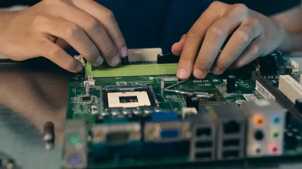
Component Placement
After solder paste, parts are put on the PCB. Machines do this fast. They do it right. New assembly lines use good tools.
Pick-and-Place Machines: These machines pick parts. They pick from feeders. They put them on paste-covered pads.
Chip Shooters: These are fast. They place small, simple parts.
Flexible Placement Machines: These are exact. They are good for big or complex parts. Samsung/Hanwha machines are top tools. They place all sizes of parts. They are very fast. They are very exact.
Surface Mount Technology (SMT) Assembly: This way makes small boards. It makes dense boards. It is exact. It is fast.
Through-Hole PCB Assembly (THT): This way puts parts with wires. Wires go into holes. This makes strong links. It is for heavy parts. It is for old PCB designs.
Machines and robots also move parts. They make parts. They cut labor costs. They find mistakes. AI robots are very exact. They give good info. Putting parts in the right spot is key. Spacing is key. This stops shorts. It stops open circuits.
Soldering Processes
All parts are on. The PCB goes to soldering. Here, solder paste melts. It makes lasting links. These are electric and strong. Two main ways are reflow soldering. And wave soldering.
Aspect | Reflow Soldering | Wave Soldering |
|---|---|---|
Advantages | Fast joining, steady quality, works with many parts (SMT, exact parts), joins dense parts | Fast joining (for through-hole parts), cheap (for many THT), strong (even joints for THT) |
Disadvantages | Costly machines, needs high heat control, some parts can get too hot | Not for small SMT, can harm bottom SMT, thin PCBs can get too hot |
Applicability | Small electronics, SMT assembly, exact parts, bendy PCB designs | Big, dense electronics (power boards, motherboards), very strong links |
Reflow Soldering: This is mainly for SMT parts. The PCB goes through an oven. The oven has many heat zones. It slowly gets hotter. This melts the solder paste. Then, it cools the board. This hardens the solder. Convection ovens use hot air. This heats evenly. Infrared ovens heat faster. Vapor phase ovens heat very evenly. This is for heat-sensitive boards. Reflow soldering is good for new designs. It is good for small SMT parts.
Wave Soldering: This is usually for through-hole parts. The PCB goes over melted solder. The solder sticks to part wires. It sticks to PCB pads. This makes strong links. Wave soldering costs less for PTH assembly. It makes THT parts very strong.
Both ways need careful heat control. This makes good solder joints. It stops damage to parts.
Inspection and Quality Control
After soldering, the PCB is checked. This finds any mistakes. It finds assembly errors. Finding problems early saves money.
Solder Paste Inspection (SPI): This checks solder paste. It checks on the bare PCB. This is before parts are placed. It uses lasers or cameras. It measures paste amount. It measures area and shape.
Automated Optical Inspection (AOI): This system uses good cameras. It scans the board. It compares it to a perfect board. It finds part placement errors. It finds solder joint errors. New 3D AOI measures paste height. It measures volume and shape. AOI is key for quality in SMT assembly.
Automated X-ray Inspection (AXI): This system does a ‘CT scan’. It looks for hidden problems. It is good for parts like BGAs. Their solder joints are hidden. Advanced 3D AXI uses special ways. It finds small flaws. These are like empty spots. Or ‘Head-in-Pillow’ issues.
Visual Inspection: Trained people use strong magnifiers. They use microscopes. They find problems. These are like bad solder joints. Or missing parts. Or cracks. Or lifted wires.
These checks make sure assembly worked. They make sure the PCB is ready.
Testing and Validation
Testing is very important. It makes sure the PCB works. It makes sure it lasts. Many ways are used. Each checks different things.
In-Circuit Test (ICT): This is an automated way. It uses a ‘bed-of-nails’. It tests each part. It tests paths on the PCB. ICT is fast. It takes seconds. It finds many faults. It is good for mass making. It finds small part failures. But it needs costly tools. It needs special test points.
Flying Probe Testing (FPT): This needs no special tools. It uses robot arms. They test each point one by one. FPT is good for small batches. It is good for new designs. It is good for boards without test points. It costs less to start. It is good for checking designs.
Functional Test (FCT): This is the PCB‘s ‘final exam’. It checks if the PCB works. It checks in a real setting. FCT acts like the real use. It may turn on power. It checks connections. It reads sensors. FCT makes sure it works for the user. It finds problems other tests miss. These are like wrong part values. Or software errors. FCT is key for good products. It stops failures. It stops returns.
Other Tests:
Power-on self-test: Checks if the PCB turns on. It checks voltage. It checks power use. It checks parts.
Environmental stress test: Tests the PCB in different places. It checks how it works. This is under bumps. Under shaking. Under strong signals. Under wetness.
Signal integrity test: Checks how the PCB works. This is under different loads. It checks for failure. It checks for damage.
These tests check everything. They make sure the PCB is strong. They make sure it works well.
Conformal Coating and Final Assembly
The last steps often add a coating. Then, the product is put together.
Conformal Coating: This is a thin film. It covers the PCB. It protects the board. It protects from outside things.
Protection against moisture and environmental factors: It stops water. It stops dust. It stops other bad things. This makes the PCB last longer. It makes it work.
Protection against mechanical damage and abrasion: It protects from shaking. It protects from bumps. It protects from other hits.
Protection against electrical interference: It stops electric noise. This is from signals.
Increased lifespan of PCB: It protects from damage. This means fewer fixes. Fewer replacements.
Common coatings are Acrylic. Epoxy. Parylene. Polyurethane. Silicone. Each has its own good points. Silicone is bendy. It is strong. It handles extreme heat. It handles harsh places. Parylene stops water well. It stops chemicals well. It is thin. It has no holes.
After coating, the PCB goes into its case. It connects to other parts. These are screens. Batteries. Buttons. This finishes the change. It goes from a bare board. It becomes a finished electronic device.
Key Technologies in PCB Assembly for 2025
The world of electronics changes fast. New tech makes PCB assembly smarter. It makes it faster. These changes help make better products. They also make making things easier.
Automation and Robotics
Robots and smart systems are changing PCB assembly. They make the process more exact. They also make fewer mistakes. This means better products.
Surface Mount Technology (SMT): This way puts parts right on the board. It costs less. It works well. Robots make fewer errors. Robots with grabbers handle small parts. This makes stronger, smaller PCBs.
High-Density Interconnects (HDIs): These make PCBs smaller. They fit more parts in tiny spots. This means less wiring. It also makes things work better. It makes them faster. It makes them more reliable. HDIs help signals flow. They stop interference.
Advanced Materials and Manufacturing Techniques: Bendy materials help robots move in complex ways. High-frequency materials help make smaller PCBs. These materials handle heat better. They also stand up to tough conditions. This makes robots work better. Additive manufacturing makes complex designs. It does this with high accuracy. It makes things faster. It also makes less waste. This is true for small PCBs.
IoT Integration and Smart PCBs: The Internet of Things (IoT) helps robots talk to devices. It talks to sensors. This makes automated assembly safer. It makes it work better. It also makes it more flexible. For example, IoT robots in cars place parts exactly. In health care, robots like Da Vinci help with surgery. They make procedures shorter.
These steps forward make automated assembly a key part of modern making.
Miniaturization and HDI Challenges
Making PCBs smaller and denser brings new problems. High-Density Interconnect (HDI) PCBs put many features in a tiny space. This needs very careful assembly.
Challenge | Description | Solution |
|---|---|---|
Miniaturization & Component Density | Trace widths are very thin (3 mils). Spacing is also tight. Microvias (0.006 inches) make placing and drilling hard. This can cause signal loss. Or the board can fail. | Optimize Design for Manufacturability (DFM): Keep trace widths and spacing within limits. Do not put microvias too close. Make sure pad sizes are big enough. |
Soldering Difficulties | Small pad sizes. Fine-pitch components (0.4 mm BGAs/QFNs). These raise the risk of bridging. They can also cause bad joints. Uneven heat in multi-layer boards can cause cold joints. Or part damage. | Advanced Soldering Techniques: Use special reflow profiles (preheat 150-180°C, peak 235-245°C). Use Type 4/5 solder paste. Vapor phase soldering helps spread heat better. |
Component Placement Precision | Tight part packing needs very high accuracy (±0.001 inches). Small parts (0201, 01005) can have flaws. These are like tombstoning. | Enhanced Placement Accuracy: Use very exact pick-and-place machines. They have vision systems. Use custom holders. Use Automated Optical Inspection (AOI) after placing. |
Signal Integrity & Crosstalk | High trace and via density causes crosstalk. It also makes signals worse. This is true for fast uses (>1 GHz). Keeping impedance control (e.g., 50 ohms ±10%) is hard. | Ensure Signal Integrity: Design for controlled impedance. Space high-speed traces. Use ground planes. Make vias better (back-drilling). |
Manufacturing & Inspection Limitations | Complex things make old testing methods not enough. Flaws in microvias or hidden layers are hard to find. This needs costly advanced ways. Like X-ray inspection. | Advanced Inspection & Testing: Use X-ray inspection for microvias. Use it for hidden layers. Use microsectioning for quality checks. Use in-circuit testing (ICT) for connections. |
General Complexity | The whole nature of HDI PCB assembly is complex. | Partner with Experienced Manufacturers: Work with experts in microvias. Work with experts in fine-pitch soldering. Work with experts in multilayer designs. This makes sure the output is high quality. |
These answers help fix the problems. These are problems with making very small and complex PCBs.
Advanced Materials and Components
New materials and parts are making PCBs better. They make them work better. They also help the environment.
Material/Component | Description/Benefit |
|---|---|
It is light. It is cheap. It can be recycled fully. It is made from pressed paper or cardboard. It works for low-power electronics. Or throw-away electronics. | |
Cellulose PCB Substrate | It comes from plant fibers. It has good mechanical features. It has bendy strengths up to 100 MPa. It is strong. It is light. |
Sustainable PCB Laminates | These are made from plants. Or they have no halogen. They replace old laminates. They avoid bad chemicals. These are like brominated flame retardants. |
Eco-friendly PCB Coatings | These use water. Or they come from plants. They have very few bad gas releases. They are safer than coatings with solvents. |
Water-based PCB Inks | They use water as the main liquid. This lowers bad gas releases. It is better than old toxic inks with solvents. |
These materials help make more sustainable parts. They make high-performing parts for electronic devices.
Smart Factory and Industry 4.0
Industry 4.0 is changing PCB assembly. It uses smart factory ideas. It uses data analysis. It uses AI. This makes making things much better.
Smart making uses IoT and AI. It makes PCB assembly more exact. This means fewer flaws. Products get to market faster.
IoT sensors watch PCB assembly lines. They watch in real-time. They find problems right away.
AI-powered vision systems find flaws much better than people. This cuts waste by 30%.
These technologies create a very good automated assembly place. It is quick to respond. They make sure production is high quality. They make sure it is fast.
Selecting a PCB Assembly Partner for 2025
Picking the right partner is very important. This partner builds your printed circuit board (PCB). A good partner helps your product succeed. They help meet what people want in 2025. Companies must look at partners carefully.
Essential Partner Considerations
Businesses want partners with good skills. This includes fine pitch and BGA assembly. They also work with multi-layer boards. They handle high-density parts. A partner should also do Design for Manufacturability (DFM) checks. This makes sure the design works well. Experience with making test versions is good. This means quick, small orders. It also means help from engineers.
Certificates show a partner cares about quality. Look for ISO 9001 for quality. ISO 13485 is for medical devices. IPC-A-610 shows good electronic work. RoHS and REACH are also needed. A strong partner knows part suppliers well. They can suggest other parts if needed. They also stop fake parts.
Testing skills are key. This includes Functional Testing (FCT). It also includes In-Circuit Testing (ICT). Automated Optical Inspection (AOI) is important. X-ray Inspection is too. Good talking is also a must. A special project manager helps. Regular updates help too. Quick answers to questions are also key.
Different jobs have special needs. Car electronics need IATF 1649. Air and defense need AS9100. They also need ITAR. Medical devices need ISO 13485. They need FDA approval.
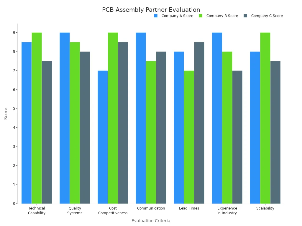
Companies can score partners. This helps them choose wisely.
Criteria | Weight | Company A Score | Company B Score | Company C Score |
|---|---|---|---|---|
Technical Capability | 25% | 8.5 | 9.0 | 7.5 |
Quality Systems | 20% | 9.0 | 8.5 | 8.0 |
Cost Competitiveness | 15% | 7.0 | 9.0 | 8.5 |
Communication | 15% | 9.0 | 7.5 | 8.0 |
Lead Times | 10% | 8.0 | 7.0 | 8.5 |
Experience in Industry | 10% | 9.0 | 8.0 | 7.0 |
Scalability | 5% | 8.0 | 9.0 | 7.5 |
Weighted Total | 100% | 8.45 | 8.40 | 7.90 |
The Role of Design for Manufacturability
A partner’s DFM skill helps product quality. It also helps cost. DFM finds design flaws early. This is before making anything. It stops costly delays. It stops wasted materials. DFM also makes products better. It makes them last longer. It helps designers and makers talk. This makes test versions faster. It makes full production faster.
DFM skill lowers making costs. It makes making and putting together easier. It lowers mistakes. This leads to better products. Well-made PCBs break less often. This means less fixing. It means less waste. It also makes more good PCBs. More usable PCBs come from each run. DFM picks and places parts well. This lowers part costs. It also lowers work and energy costs. This means more money earned.
PCB assembly changes a bare board. It makes it a working electronic device. This process has many steps. Robots and small parts change PCB assembly. This is true for 2025. Checking quality is key. Testing is key. Picking the right partner is key. These help make good products. Following design rules helps. It makes good electronics. Knowing this process helps new ideas. It helps compete in electronics. Good quality in each step is most important. This guide shows why it matters.
FAQ
What is PCB assembly?
PCB assembly makes a bare board work. It turns it into an electronic device. It puts parts on the board. It solders them. This process is very important. It makes almost all new electronics. Knowing about PCB assembly helps make products.
What common errors occur during PCB assembly?
Some errors can happen. Soldering can be wrong. This causes shorts or open circuits. Parts can be in the wrong spot. They can face the wrong way. These mistakes make devices not work. These errors need careful checking.
How do manufacturers prevent these errors?
Makers use strong quality checks. They use machines to look at boards. These are AOI and X-ray. These tools find errors early. Good tests also find mistakes. This helps stop problems. It makes things reliable.
What types of components are most common in PCB assembly?
Many parts are used. These include resistors. Capacitors are also used. Integrated circuits are common. Diodes and transistors are too. These parts do different electric jobs. They are key for the circuit to work.
What are some common PCB fabrication mistakes?
Common mistakes are wrong trace widths. Or wrong spacing. Holes can be drilled wrong. These problems hurt how the board works. They can also make assembly hard. Good design and making help avoid these.
See Also
Your Complete Handbook to the PCBA Manufacturing Process
Understanding PCBA Assembly: Essential Stages and Functionality Explained
Expert Advice for Choosing Superior PCB Assembly Service Providers
Maximize Your PCB Assembly: Practical Strategies for Enhanced Efficiency
Achieve Cost-Effective PCBA: Ten Pro Tips for Smart Assembly