Common Applications of Single-Sided PCBs
✅Consumer electronics (e.g., calculators, radios)
✅Power supplies
✅LED lighting circuits
✅Relays and sensors
✅Low-cost appliances
✅Industrial control and sensors
✅ Automotive electronics (non-core components)
✅Toys and educational products
✅ Communication equipment (low-end applications)
✅ Medical equipment (non-critical components)
✅Low-complexity electronic devices
Advantages of Single-Sided PCBs:
|
Cost-Effective
|
Lower production costs due to simple fabrication processes and reduced material requirements.
|
|
Easy Design & Manufacturing
|
Single copper layer simplifies design complexity, enabling rapid prototyping and production.
|
|
Quick Turnaround Time
|
Simplified structure accelerates manufacturing and assembly, reducing lead times significantly.
|
|
Lower Failure Rate
|
Fewer solder joints and components minimize the risk of circuit failures.
|
|
Suitable for Mass Production
|
Mature processes and low costs make it ideal for large-scale manufacturing.
|
|
Lightweight & Compact
|
Perfect for small, space-constrained devices (e.g., sensors, remote controls).
|
|
Easy Troubleshooting
|
Single-layer layout allows for straightforward fault detection and repairs.
|
|
Ideal for Low-Density Circuits
|
Works best for basic applications with minimal components (e.g., power circuits, LED drivers).
|
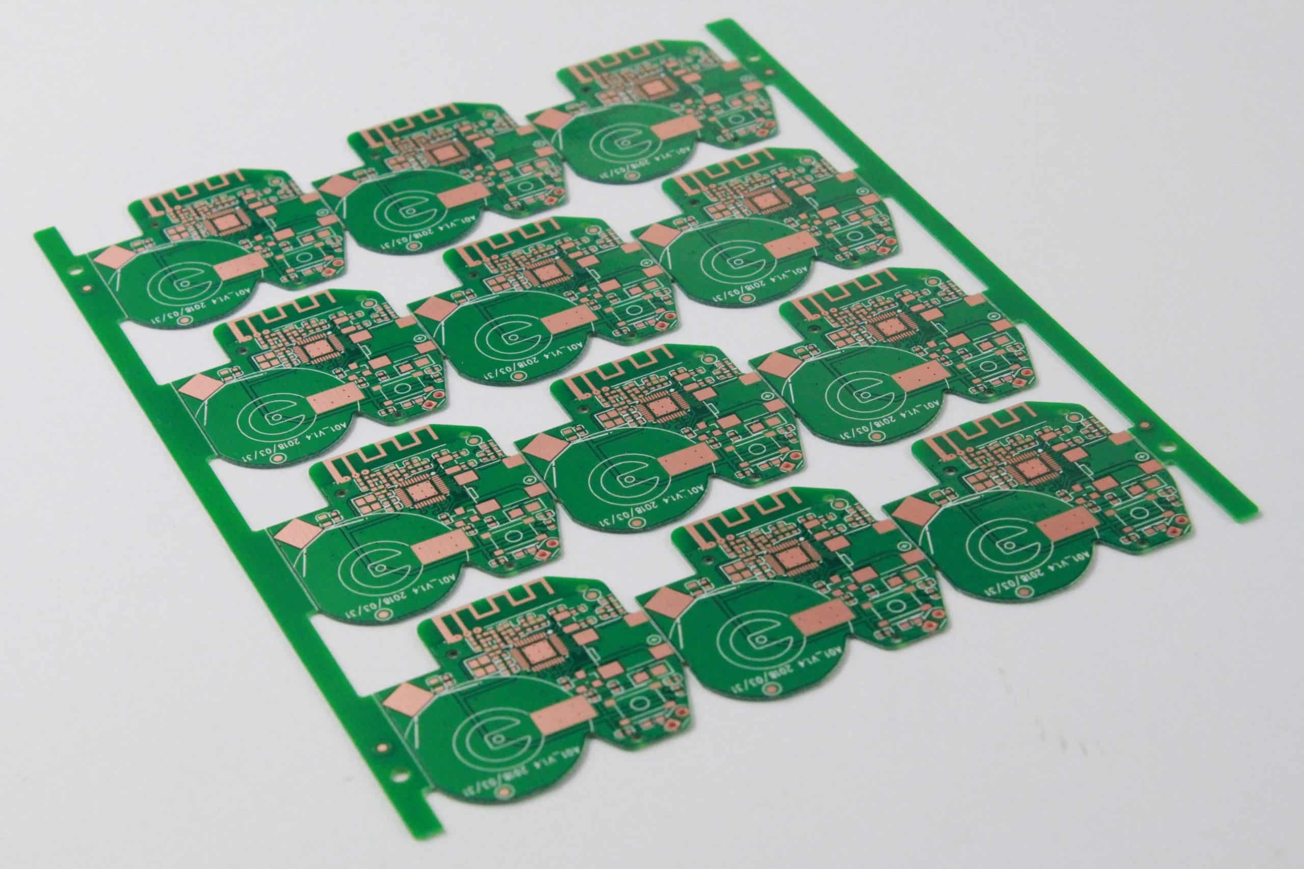
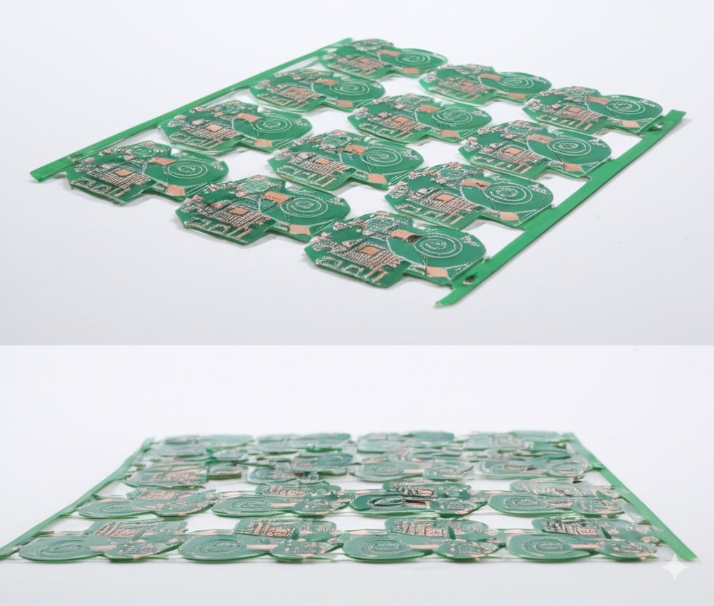
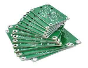
Single-Sided PCBs Manufacturing Process
The manufacturing of a Single-Sided PCB involves several key steps to create the copper traces and component mounting holes. Here’s an overview of the process:
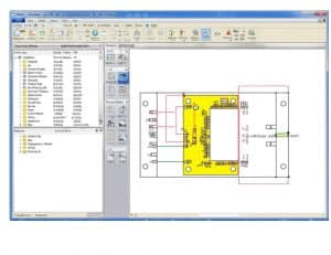
1.Design & Layout
The circuit layout is designed using PCB design software (e.g., Altium, Eagle, KiCad).
The design is checked for electrical rule compliance and manufacturability.
The finalized Gerber files are sent for PCB fabrication.
2.Substrate Preparation
The base material (e.g., FR4, CEM-1, or phenolic resin) is selected.
A thin copper layer is laminated onto one side of the board.
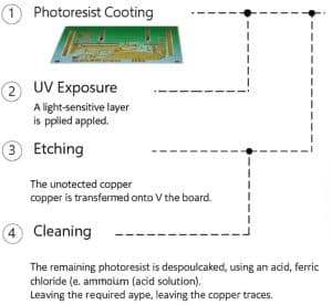
3.PCB Patterning (Etching Process)
Photoresist Coating: A light-sensitive layer is applied to the copper surface.
UV Exposure & Development: The PCB design is transferred onto the board using a UV light process.
Etching: The unprotected copper is dissolved using an acid solution (e.g., ferric chloride or ammonium persulfate).
Cleaning: The remaining photoresist is removed, leaving the required copper traces.
4.Drilling
Holes are drilled for through-hole components and mounting using CNC drilling machines.
5.Solder Mask Application (Optional)
A solder mask (protective layer) is applied to prevent oxidation and short circuits.
The mask is exposed to UV light and then developed to uncover soldering points.
6.Silkscreen Printing (Optional)
Labels, symbols, and component markings are printed onto the board.
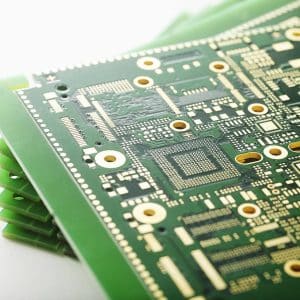
7.Surface Finishing (Optional)
Surface finishes like HASL (Hot Air Solder Leveling) or ENIG (Electroless Nickel Immersion Gold) are applied for better solderability.
8.Cutting & Profiling
The PCB is cut into final dimensions using CNC routers or V-grooving machines.
9.Inspection & Testing
Visual Inspection – To check for defects like misalignment, etching errors, or drilling issues.
Electrical Testing – Conductivity tests ensure the circuit functions as designed.
10.Final Packaging & Delivery
The PCBs are cleaned, packed, and shipped for assembly.
Reviews
There are no reviews yet.