Common Applications of Multi-Layer PCBs:
✅Computers & Servers – Motherboards, GPUs, and high-speed processors.
✅Consumer Electronics – Smartphones, tablets, and gaming consoles.
✅Telecommunication Equipment – 5G networks, routers, and satellite systems.
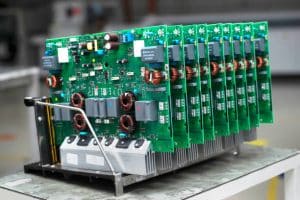
✅Automotive Electronics – ADAS, infotainment systems, and EV controllers.
✅Medical Devices – MRI, ultrasound, and wearable health monitors.
✅Industrial & Mechatronic Equipment – Robotics, automation, and power distribution systems.
Advantages of Multi-Layer PCBs
|
Higher Circuit Density
|
Allows more components and connections in a compact space.
|
|
Smaller & Lighter Design
|
Reduces PCB size for advanced, compact devices.
|
|
Improved Electrical Performance
|
Lower signal interference and better power distribution.
|
|
Increased Design Flexibility
|
Supports high-speed and high-frequency circuits.
|
|
Better Heat Dissipation
|
Evenly distributes heat across multiple layers.
|
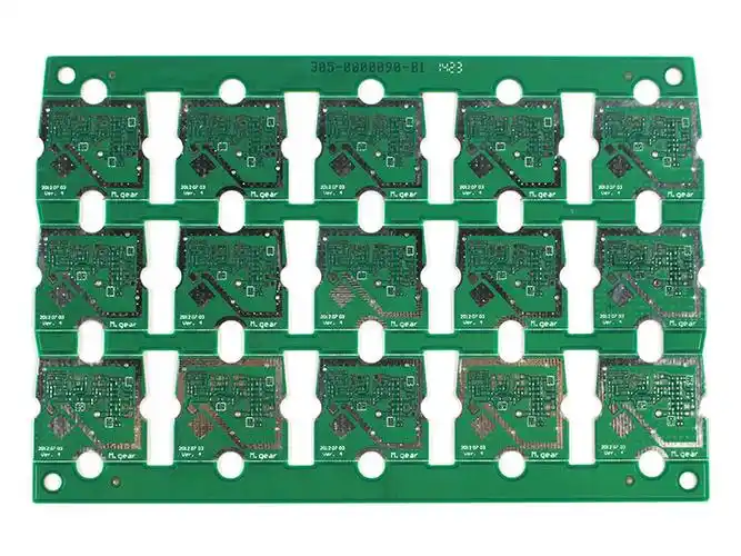
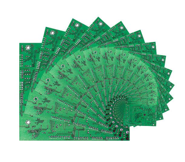
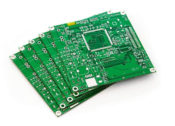
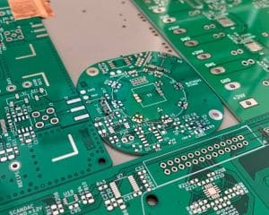
Multi-Layer PCBs Manufacturing Process
The manufacturing of Multi-Layer PCBs is more complex than single- and double-layer PCBs due to multiple copper layers and precise alignment requirements. Below is a step-by-step process:
1.PCB Design & Layout
Circuit design is created using PCB CAD software (e.g., Altium Designer, Eagle, KiCad).
The design includes multiple copper layers, vias, and power/ground planes.
Gerber files are generated for fabrication.
2.Material Selection & Inner Layer Preparation
Core Material: Usually FR4, polyimide, or Teflon for high-frequency applications.
Copper-clad laminate is cleaned to ensure proper adhesion.
Photoresist Application: A UV-sensitive film is applied to the inner layers.
3.Inner Layer Imaging & Etching
The circuit pattern is transferred onto inner layers using UV light exposure.
Etching: Excess copper is removed using a chemical solution.
Photoresist Stripping: The remaining protective layer is removed.
4.Layer Alignment & Lamination
Inner layers are aligned with the outer layers.
Prepreg (insulating layers) and core layers are stacked.
The layers are pressed together using high-temperature and high-pressure lamination.
5.Drilling (Via Hole Creation)
CNC Drilling: Creates holes for through-hole, blind, and buried vias.
Laser Drilling (for HDI PCBs): Used for micro-vias in high-density boards.
6.Plated Through-Hole (PTH) Process
Copper electroplating coats the drilled holes to create electrical connections between layers.

7.Outer Layer Imaging & Etching
Similar to inner layer etching, but applied to the outer layers.
UV exposure, etching, and cleaning to form conductive traces.
8.Solder Mask Application
Solder mask (green, blue, or black) is applied to protect the copper traces from oxidation and solder bridging.
9.Silkscreen Printing (Optional)
Labels, component markings, and logos are printed for identification.
10.Surface Finishing
Enhances solderability and protects copper:
HASL (Hot Air Solder Leveling) – Cost-effective.
ENIG (Electroless Nickel Immersion Gold) – High reliability.
OSP (Organic Solderability Preservative) – Lead-free option.
11.Profiling & Cutting
PCBs are cut into final dimensions using CNC routers or V-grooving machines.
12.Electrical Testing & Quality Control
Automated Optical Inspection (AOI) – Detects defects in PCB traces.
Flying Probe or Bed of Nails Testing – Ensures electrical continuity.
13.Final Cleaning, Packaging & Delivery
PCBs are cleaned to remove contaminants.
Inspected, packed, and shipped for assembly (PCBA) or direct use.
Reviews
There are no reviews yet.