
You use printed circuit boards every day. They are in smartphones and cars. PCB manufacturing makes these important parts. It turns your pcb design into a real board. The process has pcb fabrication and assembly steps. These steps include printing layers and etching copper. They also drill holes and place components. The global market for pcb manufacturing is over $70 billion. It keeps growing as industries want better boards. Each pcb development starts with your pcb design. It goes through many steps to make reliable products.
Key Takeaways
Printed circuit boards (PCBs) have different types. There are single-sided, double-sided, and multilayer PCBs. Each type fits different projects and costs.
The PCB manufacturing process makes your design real. It uses steps like printing, etching, drilling, and layering. These steps help make sure the board is good and works well.
Assembly puts parts on the board with machines. Soldering methods join the parts. Careful checks help stop mistakes and make strong connections.
Quality control uses checks and tests to find problems early. This helps make PCBs that work well and last longer.
Knowing about PCB types, making, and testing helps you pick better materials and ways for your projects. This leads to products you can trust and that last a long time.
Printed Circuit Board Types
There are different types of printed circuit boards in electronics. Each type of pcb has special features and is good for certain jobs. If you know about these types, you can pick the best circuit board for your project.
Single-Sided PCB
A single-sided pcb has copper traces and parts on just one side. This printed circuit board is the easiest and costs the least. You see it in simple things like calculators, remote controls, and LED lights. The design means the circuit board can only handle easy circuits. You can use this pcb when you want to make something fast and cheap.
Tip: Pick single-sided pcbs for easy circuits when you need to save money.
Double-Sided PCB
A double-sided pcb has copper on both sides of the printed circuit board. You can put parts and traces on both sides, so you can make harder designs. Plated vias link the two layers, so the circuit board works in things like smartphones and car dashboards. This pcb costs more than a single-sided pcb because it needs more steps like drilling and plating.
More space for routing
Can fit more parts
Used in harder electronics
Multilayer PCB
A multilayer pcb has three or more layers of copper and insulation. This printed circuit board is for high-density and strong circuits. You find this kind of circuit board in small devices that need lots of connections, like computers and medical tools. Multilayer pcbs give better signals and save space, but they are harder to make and cost more.
PCB Type | Layers | Typical Use Cases | Cost Level |
|---|---|---|---|
Single-Sided | 1 | Toys, LED lights, calculators | |
Double-Sided | 2 | Phones, dashboards, sensors | Medium |
Multilayer | 3 or more | Laptops, routers, medical gear | High |
Rigid, Flexible, Rigid-Flex
You can pick rigid, flexible, or rigid-flex printed circuit boards.
Rigid pcb has a hard base and works in most normal electronics.
Flexible pcb can bend and twist, so it fits in small or moving places.
Rigid-flex pcb mixes both types, so you get strength and bending in one circuit board.
Flexible and rigid-flex pcbs use special stuff like polyimide, which makes them light and tough. These types help you save space and make things last longer, especially in devices that move or shake.
PCB Manufacturing Process
You begin the pcb manufacturing process with your pcb design. This process changes your digital files into a real pcb. Each step in pcb fabrication helps make a strong product. You must follow strict rules and use new technology. This makes sure your pcb meets quality standards.
Design and DRC Checks
You start with your pcb design in special software. You make files like Gerber, drill files, and assembly drawings. These files guide the pcb manufacturing process. Before sending your design to a pcb fabrication company, you run a Design Rule Check (DRC). DRC checks if your pcb design follows rules like IPC, ISO, and UL.
It looks for signal integrity, power integrity, and electromagnetic interference.
DRC tools help you find mistakes early and save time.
You can change DRC rules for high-speed or high-voltage designs.
Using DRC during pcb design makes your product better and more reliable.
Note: Running DRC before pcb fabrication helps you avoid problems and keeps the pcb manufacturing process smooth.
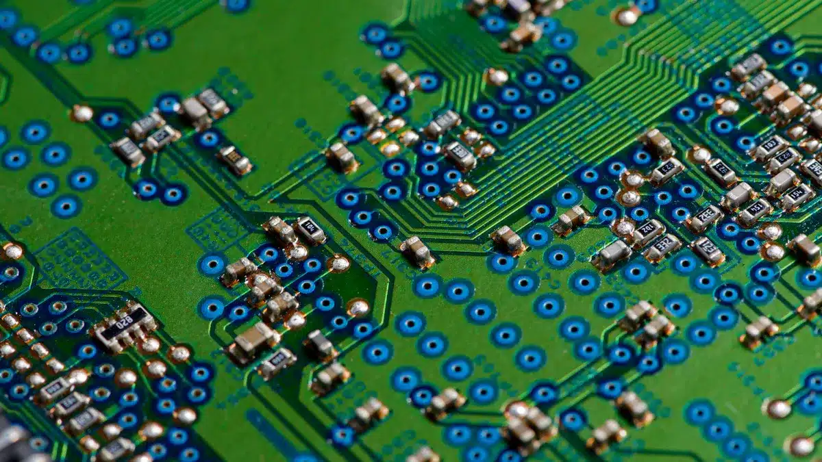
Circuit Pattern Printing
After finishing your pcb design and DRC checks, you print the circuit pattern. You use photoresist and laser direct imaging. You put copper layers on an insulating base. You cover the board with photoresist and shine UV light or lasers on it. This step hardens the photoresist where copper should stay. The soft photoresist washes away, showing extra copper. Laser direct imaging gives you clean and exact circuit patterns. This is important for modern pcb manufacturing.
Etching and Copper Removal
Next, you remove extra copper with chemical etching. You put the board in chemicals like ferric chloride, cupric chloride, or ammonium persulfate. These chemicals dissolve the exposed copper and leave the needed traces. You control heat and time to stop over-etching or under-etching.
Here is a table showing common etchants:
Etchant Chemical | Type | Characteristics and Usage |
|---|---|---|
Ferric Chloride | Acidic Etchant | Works well, used a lot, but costs more to throw away; used with photoresist. |
Cupric Chloride | Acidic Etchant | Good for small features; can be reused; needs air flow when reused. |
Ammonium Persulfate | Oxidizing Etchant | Used by hobbyists; strong oxidizer; easier to throw away than ferric chloride. |
You rinse the board after etching and take off the last photoresist. This step in pcb manufacturing shows the final copper pattern.
Drilling and Plating
You drill holes for vias and parts with computer machines. Mechanical drilling works for most holes. Laser drilling is for microvias and tiny features. You plate the holes with copper to connect layers.
The smallest mechanical drill hole is about 6 mils.
The smallest laser drill hole is about 4 mils.
The best aspect ratio for through-holes is 10:1.
You can see the drilling and plating tolerances in the chart below:
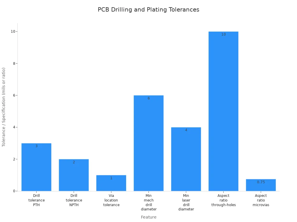
You must manage tolerances well. This step in pcb manufacturing affects how the board works and how strong it is.
Lamination for Multilayer PCB
If you make a multilayer pcb, you use lamination. You stack layers between prepreg sheets and press them with heat (180-200°C) and pressure (300-500 psi) for up to two hours. Picking the right prepreg and stack-up is important for quality. You use holes and vacuum lamination to keep layers lined up and stop air bubbles.
You check the laminated board with X-ray or optical inspection.
You test for heat stress and bonding problems before making more boards.
Tip: Vacuum lamination stops air bubbles and keeps layers together, making your multilayer pcb stronger and better.
Solder Mask and Silkscreen
You put a solder mask on to protect copper traces and stop solder bridges. You use stencils or photoimageable masks to make openings for soldering. The solder mask covers the board except for pads for parts. This layer also gives electrical insulation, so traces can be closer.
After the solder mask cures, you print the silkscreen layer. You use non-conductive ink to add part outlines, names, and polarity marks. The silkscreen helps you find parts and test points during assembly and checks.
Solder mask and silkscreen layers follow IPC rules for space and print quality.
PCB design tools help you avoid mistakes in these layers.
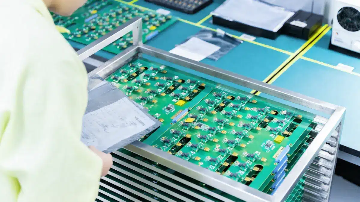
Panelization and Cutting
You group many pcbs on one panel to save time. You use V-scoring, tab routing, or routing depanelization to cut boards after pcb fabrication.
Good spacing (2.5 to 5 mm) between pcbs stops damage when cutting.
Edge clearances (about 12.7 mm) help with safe handling and tools.
V-Cut is fast and cheap but can leave burrs; tab routing is good for odd shapes and gives better results.
Here is a table comparing panelization and cutting methods:
Method | Description | Advantages | Disadvantages | Impact on Yield and Production Efficiency |
|---|---|---|---|---|
Manual Depanelization | Breaking or using pliers to separate boards by hand. | Simple, low cost (used in the past) | High risk of PCB damage from too much force | Low yield from damage; not used much now |
V-Cut (V-Scoring) | Cutting V-shaped grooves on boards for easy break with a blade. | Fast, simple, low cost, good for rectangles | Can leave burrs, only for straight cuts | Medium yield; burrs can hurt quality; good for simple shapes |
Tab Routing | Boards joined by small tabs with holes; cut by machine along edges. | Good for odd shapes, better support | Costs more, takes longer | Higher yield, less stress; good for odd shapes |
Routing Depanelization | Uses a rotary cutter to cut along set paths, straight or curved. | High-quality cuts, few burrs or stress | Slower and costs more than V-cut | High yield; less stress means less damage |
You can see the effect of depanelization methods in the chart below:
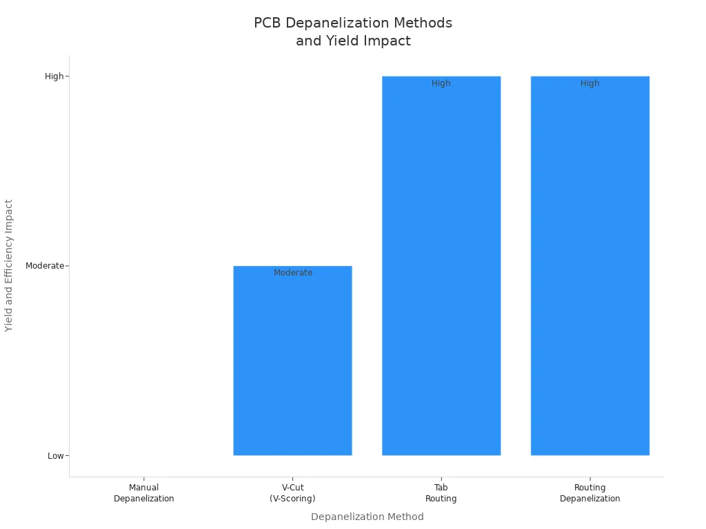
Picking the right panelization and cutting method in pcb manufacturing helps you get more boards and spend less.
Note: Good panel layouts and careful cutting help you get more pcbs from each panel and stop damage.
You finish the pcb manufacturing process by checking and testing the bare board. You look for electrical connections and shorts before assembly. The pcb fabrication process turns your pcb design files into a real pcb ready for parts.
Circuit Board Assembly
The pcb assembly process changes a plain board into a working device. You must put on parts, solder them, and fix problems to make sure your pcb works well.
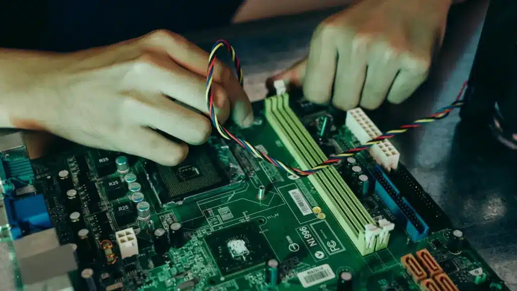
Component Placement
You begin by putting parts on the circuit board. Most factories use machines for this job. Here is how it works:
Solder paste goes on the pads with a stencil printer that lines things up.
Pick-and-place machines grab parts from tape reels, tubes, or trays. They use a vacuum or gripper nozzle.
Vision systems check each part’s spot and direction before placing it.
The machine puts each part in the right place on the pcb.
Automated Optical Inspection (AOI) checks if the parts are in the correct spots.
The board goes through a reflow oven. The oven melts the solder paste and holds the parts in place.
You can use more than one pick-and-place machine for different part sizes. This step makes sure your pcb has all the right parts in the right places.
Soldering Methods
You need to connect the parts to the board with soldering. There are different ways to do this. Each way has its own good points. The table below shows the main soldering methods used in pcb assembly:
Soldering Method | Description | Suitable Applications | Advantages |
|---|---|---|---|
Reflow Soldering | Uses solder paste and heats it in a reflow oven. | Surface-Mount Technology (SMT) | Good for small parts; uses machines; saves work; gentle heat. |
Wave Soldering | The board goes over a wave of melted solder. | Through-Hole Technology (THT) | Fast for many boards; strong joints; cheaper equipment. |
Selective Soldering | Soldering only certain spots for through-hole parts. | Mixed-technology PCBs | Very exact; does not heat the whole board; mixes machine and hand work. |
Hand Soldering | Soldering by hand with an iron and wire. | Small jobs and repairs | Flexible; cheap; good for testing and fixing boards. |
You pick the best soldering way for your board design and how many you need to make.
Assembly Challenges
You will face problems during pcb assembly. Here are some common ones and how to fix them:
Getting parts can be tough. You need good suppliers and must check for fake parts.
Bad placement or alignment can cause shorts or make the board fail. Machines and AOI help you find mistakes early.
Soldering problems like cold joints or solder bridges can happen. You fix these by watching solder heat and using good materials.
Bad board design can slow down making the board. You should follow Design for Manufacturability (DFM) rules and work with skilled engineers.
Heat control is important. Too much heat can hurt your pcb. You use heat sinks, thermal vias, and good airflow to keep the board cool.
Making small boards is harder. You need careful planning and exact machines for high-density pcbs.
Tip: Test and check your boards often. This helps you find and fix problems before your board is used.
PCB Quality and Testing
Inspection Methods
You must check every PCB for problems before it leaves the factory. This helps you find issues early and stops failures later. Here are the main ways to inspect:
Manual Visual Inspection: You use magnifiers and bright lights. You look for bad solder joints, wrong parts, or cracks.
Automated Optical Inspection (AOI): Machines use cameras to scan your board. AOI finds missing parts, bad solder, and open circuits.
X-Ray Inspection: X-rays let you see inside the board. You can find hidden problems like empty spots in solder or layers that do not line up.
Inspection Method | Defects Detected |
|---|---|
Manual Visual Inspection | Solder bridges, cracks, wrong parts |
Automated Optical Inspection | Missing parts, bad solder, open circuits |
X-Ray Inspection | Voids, internal cracks, hidden solder problems |
Tip: Always use rules like IPC-A-610 when you check your boards.
Testing Techniques
Testing makes sure your PCB works right. You use different tests to find problems:
In-Circuit Testing (ICT) checks for open or short circuits. It also measures if each part works.
Flying Probe Testing uses moving probes to find loose connections, resistance problems, and shorts.
Functional Testing turns on your board and checks if it works in real life.
Burn-In Testing puts heat and power on your PCB to find early failures.
Design for Testing (DFT) means you add test points when you design. This makes testing easier and better.
These tests help you find bad solder joints, wrong parts, or broken traces. They also show if your board can handle tough conditions.
Reliability Factors
You want your PCB to last a long time. Many things affect how strong and reliable it is:
Pick good materials like FR-4 or polyimide for strength and heat.
Use thick copper and good plating to carry more current and stop rust.
Design with the right trace width and spacing to stop overheating.
Make sure steps like drilling, etching, and plating are exact.
Add finishes like ENIG or HASL to stop oxidation.
Test your boards with heat cycles, damp heat, and salt spray to find common failures.
Note: Companies that use strict quality checks and advanced tests can lower defect rates from 0.9% to 0.14%. This means your products will work better and last longer.
You now know the main steps in pcb manufacturing. These steps go from design to picking materials, then to assembly and testing. When you learn how a printed circuit board is made, you can pick better materials and layouts for your project. Quality control and testing help find problems early. This means your products will work well and last longer. When you look at different manufacturers, check if they have good technical skills. Also, see if they have certifications and positive customer reviews.
Remember, if you understand the pcb manufacturing process, you can make better choices and get printed circuit boards you can trust.
FAQ
What is the difference between PCB fabrication and PCB assembly?
PCB fabrication makes the bare board from your design files. PCB assembly adds electronic parts to the board. You need both steps to create a working device.
How do you choose the right PCB type for your project?
You look at your device’s needs. Use single-sided PCBs for simple gadgets. Pick multilayer PCBs for complex electronics. Flexible PCBs work best in tight spaces or moving parts.
Why do you need a solder mask on a PCB?
A solder mask protects copper traces from damage. It stops solder bridges and keeps your board safe during assembly. You get better reliability with a good solder mask.
What tests help you check PCB quality?
You use visual inspection, AOI, and X-ray to find defects. In-circuit and functional tests show if your board works. These steps help you catch problems before shipping.
Can you reuse a PCB after removing components?
You can reuse a PCB if you remove parts carefully. Check for damaged traces or pads. Clean the board before adding new parts. Reusing works best for prototypes or repairs.
See Also
Understanding PCBA Manufacturing And Its Importance Today
Step-By-Step Guide To The PCBA Manufacturing Process
The Role Of PCBA Services In Electronics Production