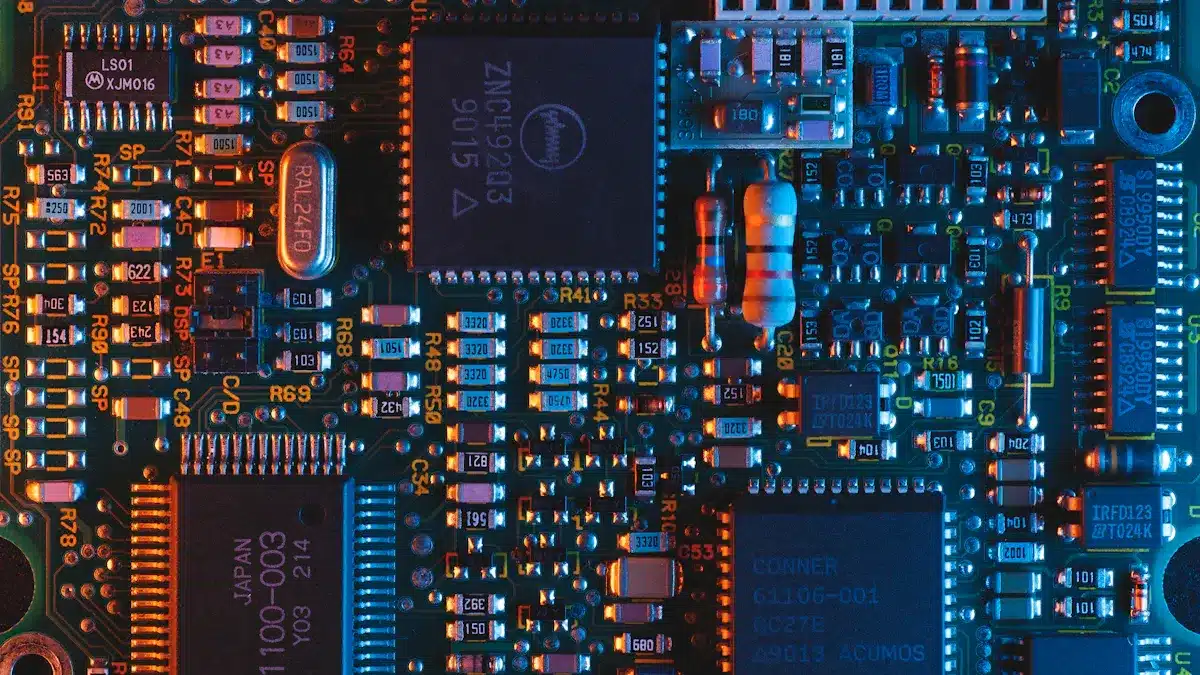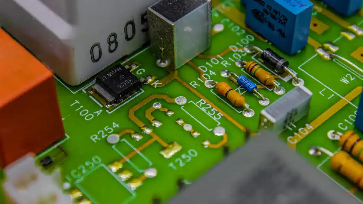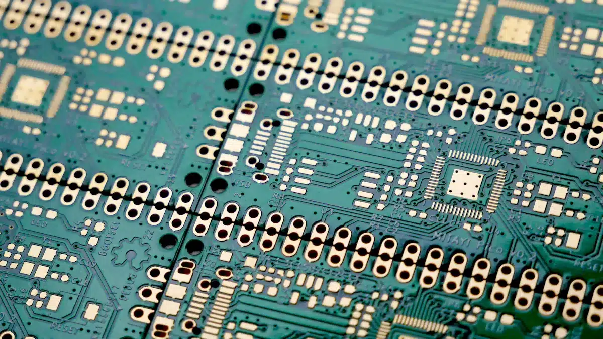
Printed circuit boards (PCBs) are very important in today’s electronics. You can find them in devices like smartphones and computers. These boards connect electronic parts. They help devices work correctly. The pcb fabrication process is key to making these important parts. It has many steps that make sure they are good quality and reliable.
Market Growth Reports say the global Printed Circuit Board market is about USD 82.25 billion in 2024. This amount is expected to rise to around USD 113.73 billion by 2033. This shows how important the industry is. The pcb manufacturing process has steps like design, choosing materials, and putting things together. Each step helps the final product work well and last long.
Key Takeaways
Good PCB design is very important. It helps avoid mistakes that can lead to problems and slow down production.
Picking the right materials, like FR-4 for the base and copper for wires, makes PCBs work better and last longer.
Every step in making the PCB, like cutting, drilling, and plating, needs to be done carefully. This ensures good quality and reliability.
Checking everything before production, like looking over files and checking design rules, helps stop expensive mistakes.
Putting together and testing the PCB, using methods like Automated Optical Inspection and In-Circuit Testing, makes sure the final PCB works well.
PCB Design
Designing a printed circuit board (PCB) is an important step in making it. You need to be accurate in your designs to get good results. Mistakes in the design can cause big problems during making, which can hurt the quality and dependability of the final product.
Schematic Design
Schematic design is like the plan for your PCB. It shows how the electrical parts connect. This step is very important because it sets up the layout design. You should watch out for these common mistakes during schematic design:
Missing or wrong power sources.
Wrong pin definitions for programmable parts.
Unconnected nets that can stop important functions.
Signal problems like crosstalk and electromagnetic interference (EMI).
Experts say that careful PCB design that matches manufacturing needs is key for better quality and dependability. For example, making sure track widths and gaps fit copper thickness needs cuts down on mistakes. As parts get smaller, designs get more complex, so accuracy is even more important.
To avoid mistakes, you can use several strategies:
Check power nets carefully.
Talk early with teams for programmable parts.
Do systematic reviews of schematics to find common errors.
By using these tips, you can greatly lower the chances of mistakes in your schematic design.
Layout Design
After finishing the schematic design, you start layout design. This step is about placing the parts on the PCB and connecting them. The layout design affects signal quality and electromagnetic compatibility. Here are some important things to think about:
Place parts in order from input to output to reduce noise and delay.
Group similar parts together to improve function and signal quality.
Keep enough space between parts to prevent shorts and meet manufacturing rules.
Keeping solid reference planes without breaks is very important. Gaps in ground planes can mess up the return current path, raising loop inductance and making the PCB act like an unwanted antenna. This can increase EMI and lower signal quality.
You should also think about heat management by spacing out heat-producing parts. Good placement helps keep both signal quality and EMC. For example, decoupling needs for EMI are stricter than for signal quality, showing the need for careful power supply noise control.
Using advanced design methods like Design for Reliability (DFR) and Design for Manufacturability (DFM) can improve your layout. These methods help reduce PCB failures by adding reliability ideas early in the design. Techniques like failure mode analysis and simpler designs can lead to fewer product failures and lower warranty costs.
By focusing on these layout design aspects, you can make a PCB that meets both performance and reliability needs.
Pre-Production Engineering
Before starting production, you need to check your design files and engineering needs. This step makes sure everything is correct and ready for making. Here are some important things to look at:
Fabrication files: These include Gerber files, NC drill files, IPC-2581, and ODB++ for bare-board production.
Assembly files: You need the Bill of Materials (BOM) and pick-and-place files for placing parts correctly.
Prints and drawings: These show what is needed for both fabrication and assembly.
STEP files and 3D prints: Use these for how parts should be placed and to check assembly.
Testpoint reports: These show where to test for electrical and in-circuit testing.
Miscellaneous files: Include schematics, netlists, mechanical layers, and photoplot files.
Binaries and testing documentation: Important for testing in high-volume manufacturing.
You should also do a Design for Manufacturability (DFM) review. This review checks clearances, sizes, and spacing to make sure your design fits manufacturing needs. Fabrication notes should say what materials, surface finishes, impedance needs, and stack-up details are required.
Next, make sure your schematic and layout databases match. Differences between these can cause delays in production. Common problems include data that does not match and wrong part numbers. These mistakes can confuse manufacturers and make them ask for clarifications. This can slow down production and raise costs.
To avoid these issues, follow these steps:
Check schematic drawings and BOM before building the layout.
Compare schematics and circuits visually after finishing the design.
Run design rule checks (DRC) to check layer stack-up and part placement.
Clean up the PCB layout to fix any errors found.
Review production files for completeness before sending them to fabrication.
By carefully checking your design files and syncing your databases, you can reduce mistakes and make the move to production smoother. This careful work leads to a more reliable and efficient PCB manufacturing process.
Material Selection

Picking the right materials for your PCB is very important. The materials you choose affect how well it works, how long it lasts, and how much it costs. There are two main types of materials: substrate materials and conductive materials.
Substrate Materials
Substrate materials make up the base of your PCB. They give support and keep electricity from leaking. The most common substrate material is FR-4. It makes up about 75% of the market. This material is made of woven fiberglass and epoxy resin. It has a good mix of electrical, mechanical, and thermal properties, which makes it useful for many uses.
Here’s a quick look at substrate materials and their market shares:
Substrate Material Type | Market Share (%) | Notes |
|---|---|---|
Rigid PCB Substrates (FR-4) | 75% | Most commonly used; known for balanced properties |
Flexible PCB Substrates | 25% | Fastest growing segment; driven by wearable electronics |
Different substrate materials can change how heat and electricity work. For example, Insulated Metal Substrates (IMS) are great for getting rid of heat. They are perfect for power electronics. On the other hand, ceramic substrates have high thermal conductivity, which is good for high-frequency uses. Choosing the right substrate helps control heat and protects the parts.
Conductive Materials
Conductive materials are key for sending electrical signals through your PCB. The main conductive material is copper. It is cheap and has great electrical conductivity. Here are some benefits of common conductive materials:
Copper: High conductivity, low cost, good thermal conductivity.
Silver: Best conductivity, does not rust, but is expensive.
Gold: Does not corrode and is reliable, but very costly.
In high-frequency uses, the choice of conductive material can greatly affect performance and cost. For instance, PTFE has great electrical properties but makes manufacturing harder and more expensive. Finding a balance between performance and cost is important, especially for big projects like 5G networks.
Choosing the right materials for your PCB improves performance and ensures reliability and cost-effectiveness. By knowing the properties of substrate and conductive materials, you can make smart choices that lead to successful PCB fabrication.
PCB Manufacturing Process

The pcb manufacturing process has several important steps. These steps change your design into a working printed circuit board (PCB). Each step is important for making sure the final product is good quality and reliable. Let’s look at the main stages in this process:
Board Cutting
The first step is board cutting. You start with a big sheet of substrate material. Then, you cut it into smaller pieces that match your design. Being precise is very important here. Industry rules say that board thickness can vary based on how it will be used. For example, boards thinner than 1.0 mm need a tolerance of ±0.10 mm. Thicker boards can have tolerances up to ±0.25 mm. This accuracy makes sure your PCB fits well in its intended use.
Inner Layer Imaging
Next is inner layer imaging. In this step, you put a photo-sensitive film on the substrate and expose it to ultraviolet (UV) light. The UV light hardens the film in certain areas. This creates a pattern that shows the copper pathways. Good inner layer imaging is key for keeping signal quality and avoiding problems like shorts or opens. High-quality imaging helps reduce mistakes in manufacturing, which saves time and money.
Etching
After imaging, the PCB goes through etching. In this process, you remove extra copper using chemical baths. Common chemicals used are ferric chloride and cupric chloride. These chemicals can be harmful to the environment, so many manufacturers are switching to safer options. Good etching makes sure only the needed copper stays, forming the right circuit patterns.
Photoresist Stripping
Once etching is done, you strip away the leftover photoresist. This step cleans the board and gets it ready for the next phase. Proper photoresist stripping is important to make sure no residues get in the way of the next steps.
Automated Optical Inspection (AOI)
Next, you do Automated Optical Inspection (AOI) to check for problems. This technology scans the PCB for issues like soldering mistakes, misaligned parts, and surface flaws. Common problems found during AOI include not enough solder, solder bridges, and lifted leads. Finding these issues early helps avoid expensive rework later in the manufacturing process.
Lamination
Lamination is the next step. Here, you bond several layers of the PCB together. This usually involves applying heat and pressure to activate the prepreg material. This fills gaps and removes air bubbles. Typical lamination temperatures are between 170°C and 180°C, with pressures from 200 to 400 PSI. Good lamination ensures the PCB is accurate in size and strong.
Drilling
Drilling is a key step where you make holes for vias and mounting components. Computer-controlled drills ensure precision. They can create microvias with diameters as small as 75 μm. This accuracy is very important for high-density interconnect (HDI) PCBs, where tight spacing is needed.
Electroless Copper Deposition
After drilling, you do electroless copper deposition. This process puts a uniform copper layer on the walls of the drilled holes. This creates a conductive pathway. High-quality electroless plating is crucial for reliable electrical connections. Poor plating can cause open circuits or delamination during soldering, which can hurt the PCB’s performance.
Profiling
Finally, profiling shapes the PCB to its final size. Techniques like laser cutting and router cutting achieve precise tolerances. Laser cutting can reach tolerances as tight as ±0.001 inches, making it great for high-end uses. Proper profiling ensures that the PCB fits well in its assembly and keeps its electrical performance.
By knowing each step of the pcb manufacturing process, you can see how they help the final product’s quality and reliability. Each phase needs careful attention to detail to make sure your PCB meets the right specifications and works as it should.
Assembly and Testing
The assembly and testing phase is very important in making PCBs. This stage makes sure your PCB works well and meets quality rules. You will go through several key steps during this process.
Component Placement
First, you need to place parts correctly on the PCB. Being precise is very important here. Industry rules say that placement tolerances should be around ±0.025 mm to ±0.05 mm. Automated pick-and-place machines help with this accuracy. These machines can keep placement accuracy within ±0.01 mm using advanced vision systems.
But, there can be challenges. Misaligned parts can cause shorts or failures. To avoid these problems, you should regularly calibrate your machines and use Automated Optical Inspection (AOI) to check component positions. This step helps catch mistakes early, ensuring a reliable assembly.
Soldering
Next, you will solder the parts to the PCB. This process connects the parts both electrically and mechanically. You must watch soldering temperatures closely. Wrong temperatures can cause defects like cold solder joints or solder bridges. Using automated soldering machines can improve quality and consistency.
Quality checks are very important during this step. You should do In-Circuit Testing (ICT) to check each part and solder joint. This testing simulates real-world conditions to confirm the PCB’s performance.
Final Inspection
Finally, you must do a careful inspection of the assembled PCB. This step ensures that everything meets quality standards before shipping. There are different inspection methods available:
Inspection Method | Description | Purpose / Defect Detection |
|---|---|---|
Component Inspection | Checks specifications and sizes of parts before assembly. | Prevents defects from damaged or wrong parts. |
Automated Optical Inspection (AOI) | Uses high-resolution cameras to check part placement and solder joints after soldering. | Finds missing parts, misalignments, and soldering defects. |
In-Circuit Testing (ICT) | Probes assembled PCBs to check connections and part function. | Tests electronic function and performance of PCB assemblies. |
By using these inspection methods, you can make sure that your finished PCBs are reliable and ready for use. This thorough approach to assembly and testing helps keep high standards in PCB fabrication.
The PCB fabrication process has important steps. These steps help make sure your printed circuit board works well and is reliable. Each part plays a special role in the final product:
Solder mask application keeps copper traces safe and boosts board reliability.
Silkscreen application helps with assembly and fixing problems by showing clear markings.
Electrical reliability testing checks that the PCB matches design specifications.
Quality checks find defects early, making sure it performs well.
By knowing these steps, you can see how complex PCB fabrication is. If you have questions or want to learn more about certain parts, feel free to explore further!
FAQ
What is a PCB?
A PCB, or printed circuit board, connects electronic parts. It gives a physical structure and electrical paths for devices like smartphones and computers.
Why is PCB design important?
PCB design is very important because it affects how well the board works and how reliable it is. Accurate designs stop problems during making and ensure it works correctly.
What materials are used in PCBs?
PCBs usually use substrate materials like FR-4 and conductive materials like copper. These materials affect how well the board works electrically and how long it lasts.
How does the PCB manufacturing process work?
The PCB manufacturing process has several steps, like cutting, imaging, etching, and assembly. Each step changes the design into a working circuit board.
What testing methods ensure PCB quality?
Common testing methods include Automated Optical Inspection (AOI), In-Circuit Testing (ICT), and visual checks. These methods help find problems and make sure the PCB meets quality standards.
See Also
An In-Depth Overview of PCBA Production Stages
Detailed Stepwise Instructions for PCBA Assembly Workflow
Key Phases Involved in PCBA Production Process
