
Printed circuit boards (PCBs) are essential for modern electronics, and understanding the printed circuit board manufacturing process is crucial to appreciating their quality and performance. This process connects different components to ensure devices function properly. High-quality PCBs guarantee stable electrical connections, which help reduce signal loss and interference. By learning about the printed circuit board manufacturing process, you can better understand how durable and efficient your electronic devices truly are.
Key Takeaways
Begin making a PCB by designing a clear plan. This helps with accurate and efficient manufacturing.
Pick the right materials for the base and wires. This balances cost, strength, and electrical performance.
Carefully follow steps for etching, layering, drilling, and plating. This builds strong and reliable circuit boards.
Place parts carefully using modern methods like Surface Mount Technology. This makes assembly faster and more accurate.
Test PCBs thoroughly using different methods. This helps find problems and ensures the device is reliable and of good quality.
Design Process
The pcb design process starts with two important steps: schematic entry and layout design. These steps turn your ideas into a printed circuit board that can be made.
Schematic Entry
You begin with schematic entry. Here, you make a visual picture of your circuit. This step includes defining parts, connections, and how they relate. You can use different software tools for this job. Here are some popular choices:
Software Tool | Key Features & Suitability |
|---|---|
Altium Designer | Easy to use, has a user-friendly interface, and 3D views; liked by experts. |
Autodesk EAGLE | Simple interface, works with Fusion 360; great for small companies. |
KiCad EDA | Free to use, open-source, good for beginners and small businesses. |
After making the schematic, you bring the parts into a new PCB document. This step decides the board’s shape, size, and layers. You connect the schematic to the PCB layout using Engineering Change Orders (ECO) to keep everything consistent. This connection is very important for keeping accuracy during the pcb manufacturing process.
Layout Design
Next, you go to layout design. This part is about placing parts on the board and connecting them with traces. Here are some key things to think about during layout design:
Component Placement and Orientation: Place parts to avoid problems and keep space from PCB edges. Keeping the same direction makes manufacturing easier.
Routing Best Practices: Reduce signal problems by spacing traces and not routing them parallel. Use solid power and ground planes to lower electromagnetic noise.
Testing Importance: Add testing steps early to find mistakes and make sure the product is ready.
By following these tips, you improve how easy it is to make and how well your printed circuit board works. The layout design step is very important to make sure your PCB meets electrical needs and works correctly.
Material Selection for PCB
When you make printed circuit boards, picking the right materials is very important. The materials you select affect how well your PCBs work, how long they last, and their cost. There are two main types of materials: substrate materials and conductive materials.
Substrate Materials
Substrate materials are the base of your PCB. They give support and keep electricity from leaking. Here are some common substrate materials and what they do:
Substrate Material | Properties | Typical Applications |
|---|---|---|
FR-4 | Strong, good at insulating, and resists fire | Consumer electronics, industrial devices |
Polyimide | Flexible, great electrical features, works in many temperatures | Wearables, aerospace, medical electronics |
Alumina (Al2O3) | Good at conducting heat, strong insulation, high temperature use | LED boards, medical circuits |
Aluminum Nitride (AlN) | Strong against heat, low expansion | High-power LEDs, sensors |
These materials have different abilities to handle heat and electricity. For example, FR-4 is popular because it balances cost and performance well. If you need something flexible, polyimide is a great option. The insulation properties of these substrates are also very important for keeping signals clear. A lower insulation value helps keep signal quality high, especially for fast signals.
Conductive Materials
Conductive materials are key for making the electrical paths on your PCB. The most common one is copper. It has great electrical flow and is not too expensive. Here’s how different conductive materials compare:
Material | Electrical Conductivity (S/m) | Cost | Advantages | Disadvantages |
|---|---|---|---|---|
Copper | Medium | High conductivity, low cost | Can oxidize over time | |
Silver | 6.3 × 10^7 | High | Best conductivity | Expensive, can tarnish |
Gold | 4.52 × 10^7 | Very High | Resists corrosion, very reliable | Very expensive |
Copper is still the best choice for most printed circuit boards because it balances performance and cost well. Silver and gold have better conductivity, but their high prices limit their use to special cases.
PCB Manufacturing Process
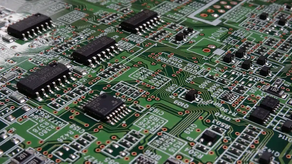
The pcb manufacturing process changes your designs into real printed circuit boards. This process has several important steps, like etching, layering, drilling, and plating. Each step needs to be done carefully to make sure the final product is good quality.
Etching and Layering
Etching is a key step in the pcb manufacturing process. It shapes the copper traces on your PCB by removing unwanted copper. Here’s how it works:
Preparation: First, you put a special film on the copper board. This film protects the areas where you want to keep copper.
Exposure: You shine UV light on the board through a mask with your design. The light hardens the film in the areas you want to keep.
Developing: After exposure, you wash the board to take off the unhardened film, showing the copper underneath.
Etching: You dip the board in an etchant solution. This solution takes away the exposed copper, leaving the desired traces.
Tip: Things like etchant concentration and temperature can change the quality of the etching. Proper control stops problems like undercutting and over-etching, which can harm trace accuracy.
Layering is another important part of the pcb manufacturing process. It means stacking layers of substrate and copper to create complex boards. Here are the steps involved:
Layer Alignment: You align the layers carefully using registration holes. This alignment is important for making sure all layers connect correctly.
Lamination: You apply heat and pressure to bond the layers together. This step needs careful control to avoid delamination, which can cause board failure.
Drilling: After layering, you drill holes for vias and component leads. Accurate drilling is very important to keep everything in the right place. You use CNC machines to ensure precision, with drill bits that have minimal run-out.
Drilling and Plating
Drilling is a key step in the pcb manufacturing process. It makes holes for electrical connections and mounting components. Here’s what you need to know:
Precision Standards: You must keep high precision during drilling. The true position of each hole is calculated to avoid misalignment. Using pilot drills helps reduce tool deflection, ensuring clean, burr-free holes.
Drilling Parameters: The smallest finished hole size for plated through holes (PTH) is usually 0.006 inches. The aspect ratio for through holes should be 10:1, meaning the depth should be ten times the diameter.
After drilling, you move on to plating. Plating is important for making conductive pathways between layers. Here’s how it works:
Cleaning: You clean the drilled holes to remove any dirt. This step ensures good adhesion of the plating material.
Electroplating: You use an electroplating process to add copper onto the walls of the holes. This creates a continuous conductive pathway.
Surface Finish: Finally, you apply a surface finish to improve solderability and protect against oxidation. Common finishes include HASL (Hot Air Solder Leveling) and ENIG (Electroless Nickel Immersion Gold).
Note: The quality of plating directly affects electrical connectivity and durability. Proper plating ensures strong mechanical support for component leads and enhances overall board performance.
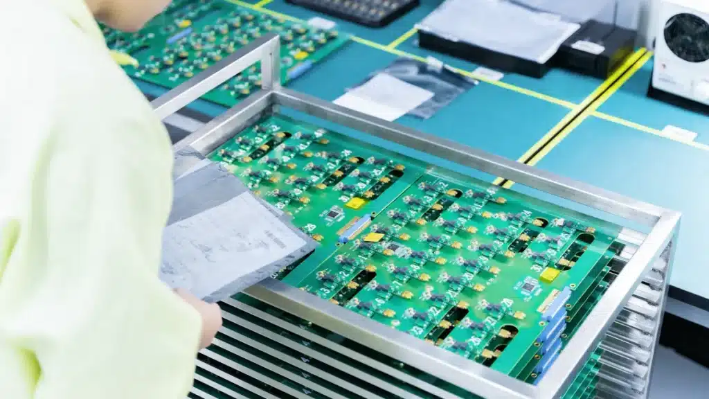
Assembly and Testing
The assembly and testing phase is very important in the PCB manufacturing process. This stage makes sure that all parts of the circuit board are placed correctly. It also checks that the final product works as it should. Quality checks during this phase can greatly affect how reliable your electronic devices are.
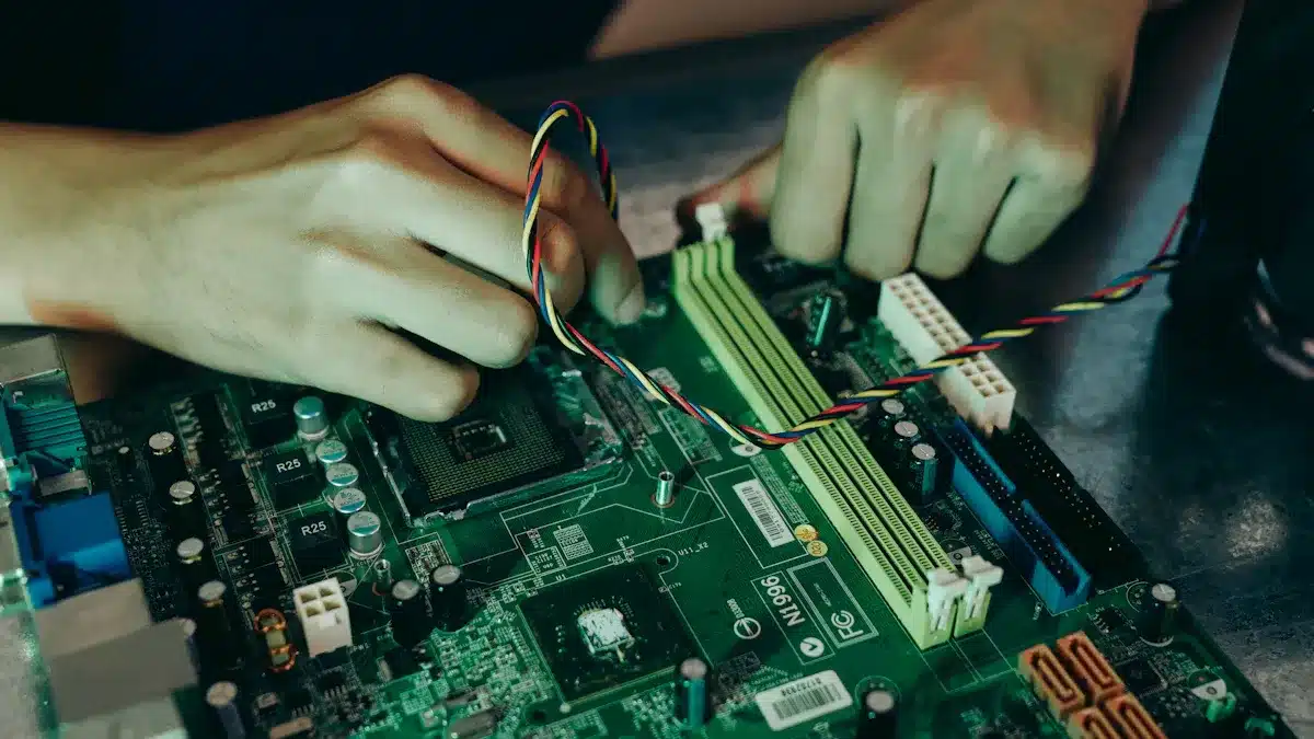
Component Placement
During the component placement process, you attach different parts to the PCB. This step is crucial because wrong placement can cause problems. Here are the most common assembly techniques:
Assembly Technique | Description |
|---|---|
Through-Hole Technology (THT) | Components with leads go through PCB holes and are soldered on the other side. Used for larger parts. |
Surface Mount Technology (SMT) | Components are soldered directly onto the PCB surface using solder paste. This allows for fast assembly. |
Mixed Technology | A mix of SMT and THT used for complex designs needing both types of components. |
Surface Mount Technology (SMT) is the most popular method today. It lets you attach parts directly to the PCB surface using solder paste and reflow soldering. This method is better than traditional through-hole techniques and is great for small and delicate parts.
Automated pick-and-place machines speed up and improve the accuracy of component placement. These machines can place parts very precisely, often within ±0.01mm. They can also place up to 200,000 components per hour, which is much faster than doing it by hand. Regularly calibrating these machines helps keep them accurate and reduces mistakes.
However, mistakes can still happen during component placement. Common problems include:
Incorrect Component Orientation: Parts placed the wrong way can cause bad connections.
Misaligned Components: Misalignment can lead to soldering problems and affect performance.
Insufficient Component Clearances: Parts too close together can cause shorts or damage.
To avoid these mistakes, you should carefully align, space, and orient the components. Grouping similar parts and keeping a consistent direction can help with assembly and testing.
Testing Methods
After assembly, you need to check if the PCB works correctly. Different testing methods help ensure that the assembled board operates as it should. Here are some main testing methods used in the PCB testing process:
Automated Optical Inspection (AOI): This method uses cameras to check component placement and solder quality without powering the board.
In-Circuit Testing (ICT): This method tests electrical connections and component placement using a bed-of-nails fixture. It finds manufacturing defects well.
Functional Testing (FCT): This method powers the PCB to check its operation, including firmware and communication buses.
Flying Probe Testing: This method uses robotic probes to measure electrical parameters without a custom fixture, making it good for low-volume runs.
Functional testing is especially important because it simulates real-world conditions. It helps find defects that other tests might miss. In contrast, in-circuit testing looks at individual parts and connections early in the manufacturing process.
Tip: Using different testing methods together can improve the overall quality of your PCB. For example, using both ICT and FCT can help make sure your board meets both component-level and functional needs.
By understanding the assembly and testing processes, you can see the effort put into ensuring the reliability of your electronic devices. Quality checks during these stages are key to delivering products that work as expected.
In short, the PCB manufacturing process has important steps that affect the final product’s quality. You begin with choosing materials, making sure to pick the right substrates and conductive materials. Then, careful techniques like etching, drilling, and plating create the paths for electrical connections. After that, you place components and do thorough testing to check if everything works well and is reliable.
Quality control is very important during this process. It helps stop mistakes and makes sure everything meets industry standards. By paying attention to these steps, you can see how they affect the performance and reliability of your electronic devices. Remember, a well-made PCB leads to longer-lasting and more efficient devices.
Tip: Always think about how important quality is in PCB manufacturing. It can greatly affect how well your electronics work.
FAQ
What is the printed circuit board manufacturing process?
The printed circuit board manufacturing process has many steps. These steps include design, choosing materials, etching, drilling, and assembly. Each step helps make sure the PCB is good quality and works well in electronic devices.
How do you test a PCB?
You can test a PCB in different ways. Some methods are Automated Optical Inspection (AOI) and In-Circuit Testing (ICT). These methods look for problems in the circuit board parts and check that everything works right before final assembly.
What materials are used in PCB manufacturing?
Common materials used in PCB manufacturing are FR-4 for substrates and copper for conductive paths. These materials give the needed electrical insulation and conductivity for reliable performance in electronic devices.
What is the importance of the PCB assembly process?
The PCB assembly process is very important. It makes sure all the circuit board parts are placed correctly and soldered well. Good assembly affects how reliable and well the final electronic device works.
How many layers can a PCB have?
A PCB can have many layers. It can have one layer or more than 20 layers, depending on how complex the circuit design is. More layers allow for more connections and smaller designs in advanced electronics.
See Also
An In-Depth Overview Of PCBA Production Procedures
Detailed Walkthrough Of The PCBA Assembly Process
Key Phases In The PCBA Production Workflow