
The world of electronics is changing quickly. PCB board printing is very important in this change. By 2025, the PCB market size is expected to be USD 79.95 billion. It will grow at a rate of about 5.6% each year. This growth shows that more advanced technologies are needed in many industries.
Key factors like the growing electronics manufacturing in Asia Pacific and the need for reliable PCBs in North America greatly affect this trend. As technology improves, it is important to keep up with these changes.
Key Takeaways
PCB printing technology is changing quickly. The market could reach USD 79.95 billion by 2025. This shows we need better ways to make PCBs.
Traditional PCB printing gives good quality but takes a lot of time. It also has limits on design choices. On the other hand, 3D printed circuit boards can be made faster and allow for new designs.
Picking the right materials is very important for how well PCBs work. Conductive materials like copper and substrate materials like polyimide affect reliability and efficiency a lot.
New PCB printing methods have benefits. They allow for smaller designs, better signal quality, and help the environment by cutting down waste and using fewer harmful chemicals.
Future trends in PCB technology will include making things smaller, flexible designs, and using AI. These changes will improve how we make products and how well they work.
PCB Printing Types
When we talk about PCB printing, there are two main methods: traditional PCB printing and 3D printed circuit boards. Each method has its own benefits and uses. They are both important in today’s electronics world.
Traditional PCB Printing
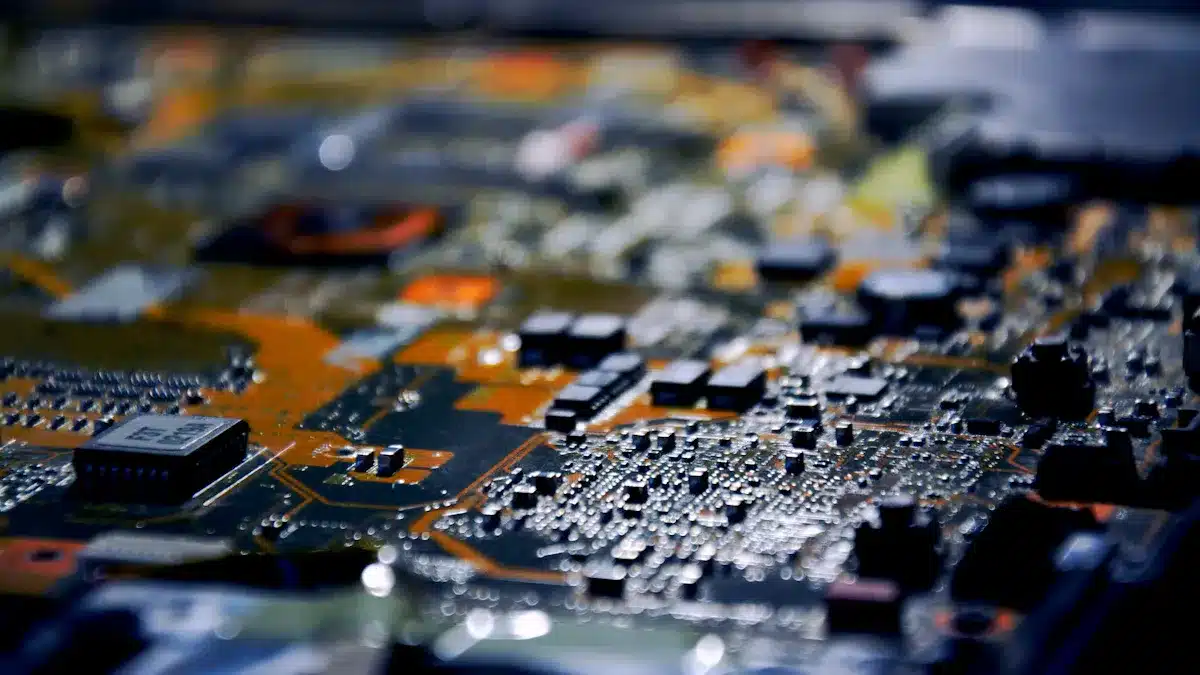
Traditional PCB printing has been used in electronics for many years. This method usually includes several steps like design, etching, and soldering. You can expect high-quality results, especially for complicated designs. However, traditional methods need special materials and can take days or even months to make one board.
Key Features of Traditional PCB Printing:
Production Speed: Takes days or months to finish.
Design Flexibility: Limited to rectangular shapes.
Material Usage: Needs specific materials, which can create waste.
Prototyping Capability: Often done by others, slowing down the process.
Output Quality: Generally high, but less flexible in design.
3D Printed Circuit Boards
On the other hand, 3D printed circuit boards are changing the industry. This new method allows for quick prototyping and design flexibility. You can make complex shapes and even flexible designs that traditional methods can’t do. The production speed is much faster, often taking 30 hours or less to finish a board.
Advantages of 3D Printed Circuit Boards:
Cost-efficient
Fast production
Design freedom
Less waste
On-demand production
High accuracy
Can create more layers
However, 3D printed circuit boards have some challenges. The materials can be limited, and their conductivity might not be as good as traditional boards. Also, the size of the boards can be limited, which may not work for all uses.
Common Applications for Each Method:
Traditional PCB Printing:
Prototyping and Design Verification: Quickly making PCB prototypes for fast testing and design checks.
Custom PCB Manufacturing: Making special PCBs for specific device needs, improving size and performance.
Electronics in Aerospace Manufacturing: Used for testing and making parts, improving quality and cutting costs.
Medical Industry: Making medical devices and models for surgeries.
Manufacturing Industry: Faster production and wider uses for complex circuits at lower costs.
3D Printed Circuit Boards:
Great for quick prototyping and custom designs.
Useful for flexible applications, like wearable devices.
Good for small production runs where traditional methods may be too expensive.
Both traditional and 3D printed circuit boards meet the needs of high-frequency and high-density electronic uses. For example, High-Density Interconnect (HDI) PCBs support compact designs and better signal quality. Flexible PCBs can bend and fit into tight spaces, while rigid-flex PCBs mix strength and flexibility for different uses.
Materials for PCB Board Printing
When you think about PCB board printing, the materials you choose are very important. They affect how well your PCBs work and how reliable they are. There are two main types of materials: conductive materials and substrate materials. Each type has special features that change how your PCBs perform.
Conductive Materials
Conductive materials are needed to create paths for electricity in your PCBs. The most common one is copper. It is famous for its great conductivity, so it is used for all traces in PCB designs. Here are some important conductive materials to know:
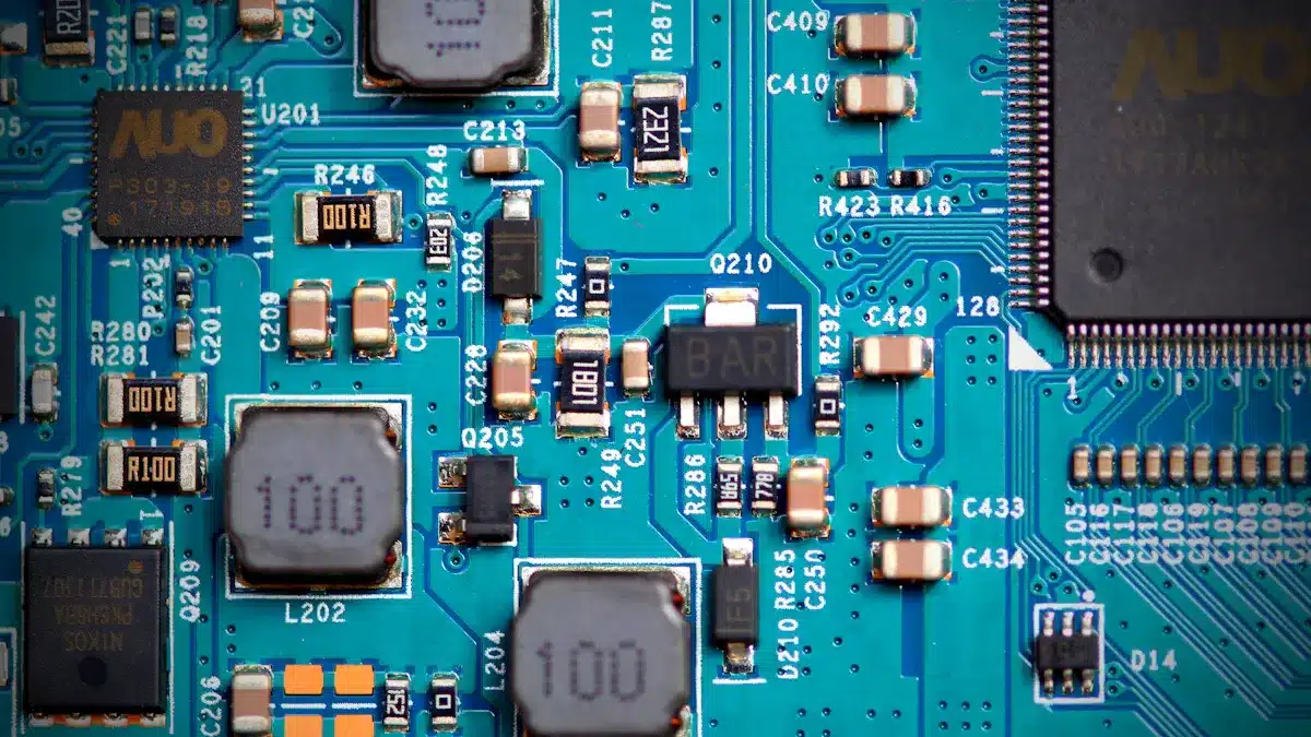
Copper: This is the main material for making PCBs. It has great electrical conductivity and is used in many applications.
Polyimide: This polymer is good for heat and flexibility. It keeps signals strong in tough places, like aerospace and cars.
PTFE (Teflon): Known for being very flexible, PTFE works well for high-frequency uses. It has a lower dielectric constant than regular materials like FR4, making it great for advanced electronics.
You can see a comparison of these materials in the table below:
Material | Thermal Conductivity (W/mK) | Dielectric Constant (Er) | Loss Tangent (Tan δ) | Volume Resistivity (Ω-cm) | Electrical Strength (V/mil) |
|---|---|---|---|---|---|
Copper | 386 | N/A | N/A | N/A | N/A |
Polyimide | N/A | 3.5 – 5.5 | 0.02 – 0.001 | 10^3 – 10^10 | 800 – 1500 |
PTFE (Teflon) | N/A | Lower than FR4 | N/A | N/A | N/A |
These conductive materials greatly affect how your PCBs work. For example, using low-loss laminates like Rogers RO4000 series can help reduce signal loss. This is very important in high-frequency uses.
Substrate Materials
Substrate materials are the base for your PCBs. They hold up the conductive paths and affect how well the board works. New improvements in substrate materials have made PCBs more efficient and reliable. Here are some important types of substrate materials:
Flexible Substrates: Made from polyimide, these can bend and fit on uneven surfaces. They are perfect for wearable devices.
Rigid-Flex Substrates: These mix flexible and rigid materials, allowing for compact designs like foldable smartphones.
Nanocomposite Materials: Adding nanoparticles makes them stronger and better at conducting heat, which improves reliability.
High-Frequency Materials: These are made for precision in high-frequency uses, boosting performance.
Choosing the right substrate material affects many things, like electrical performance, heat management, and strength. For example, FR-4 is a cheap option used a lot in consumer electronics, while high-performance materials like PTFE are needed for uses that need low dielectric constants.
You should also think about how these materials affect the environment. Making and getting rid of materials like FR-4 and copper can cause big environmental problems. Switching to lead-free solders helps lower toxicity, but these alternatives can still be hard to dispose of.
PCB Printing Processes
The PCB printing process has several important steps. These steps help make printed circuit boards successfully. Knowing these steps helps you understand how different printing methods work. Here’s a simple list of the main steps in PCB manufacturing:
Stage Number | Stage Name | Description |
|---|---|---|
1 | Circuit Board Designing | You make the design using software and print it on transfer paper. |
2 | Etching Process | This step removes extra copper from the PCB panel using a mask and special solutions. |
3 | Stripping Process | You take off the leftover copper covered by tin or lead to get a clear copper outline. |
4 | Solder Resist | Put on solder resist material to stop solder from making unwanted connections. |
5 | PCB Testing | Test the made PCB to make sure it works right using special testing tools. |
6 | PCB Assembling | Place electronic parts onto the PCB using through-hole or surface mount methods. |
Screen Printing
Screen printing is a common way to put conductive materials on PCBs. This method is cheap for making many boards. It gives high-quality results and accuracy. But it has some downsides. For example, getting the alignment just right can be hard. Also, ink can bleed, which might affect the final product. Here’s a quick look at the pros and cons of screen printing:
Advantages | Limitations |
|---|---|
Cheap for making many boards | Hard to get accurate alignment |
High-quality results and accuracy | Risk of ink bleeding |
Works for different PCB types and materials | Limited by stencil quality |
Inkjet Printing
Inkjet printing technology has changed how PCBs are made. It allows for careful application of materials, which reduces waste. The additive solder mask process only puts the mask where it’s needed, unlike older methods that cover the whole board. This saves materials and speeds up production. Inkjet printing supports detailed designs and makes sure only the right amount of materials is used.
Application | Thermal Inkjet | Piezoelectric Inkjet |
|---|---|---|
Conductive Traces | Good for wider, simpler patterns | Best for fine, detailed patterns |
Solder Mask | Works well for standard use | Great for high-resolution application |
Adhesive Deposition | Good for general use | Precise control for special adhesives |
Laser Printing
Laser printing has many benefits over other methods. It gives better resolution than traditional photolithography. This method allows for more flexible designs and faster production times. You can create detailed designs for high-density PCBs without needing phototools, which can lower circuit pattern quality.
The biggest benefit is that it is very precise. This means the final product will have clean and sharp lines and patterns.
Design files are very important in the PCB printing process. PCB layout design tools help reduce mistakes and follow design rules. They make layouts better for manufacturing. Accurate manufacturing documents are key for turning PCB designs into reliable products. This helps avoid delays and costly mistakes.
Advantages and Challenges of PCB Printing
Benefits of PCB Printing
Modern PCB printing methods have many benefits that make manufacturing better. Here’s a list of the main advantages:
Benefit | Description |
|---|---|
Compact Design | Makes devices smaller, which is important for things like smartphones and wearables. |
Reliability | Lowers connection problems because of strong designs and careful manufacturing. |
Signal Integrity | Keeps signals clear by controlling impedance and reducing interference. |
Cost-Effectiveness | Lower costs per unit when making many items because of automated processes and standard methods. |
Standardization | Makes supply chain management easier and ensures parts work together from different makers. |
Design Flexibility | Allows for unique shapes and advanced features, helping new ideas in electronic design. |
Automated Assembly Compatibility | Works well with fast assembly processes, improving efficiency and quality in manufacturing. |
Environmental Benefits | Cuts down on waste and helps recycling, supporting sustainability in electronics production. |
PCB printing also helps the environment. For example, 3D PCB printing uses only what is needed, which cuts down on waste. It uses fewer harmful chemicals and less water than older methods. Making items on demand helps avoid making too much and wasting materials. Better designs make it easier to take apart products for recycling. Plus, local production lowers transportation emissions.
Challenges in PCB Manufacturing
Even with these benefits, PCB manufacturing has some challenges. Here are some common problems:
Design mistakes can lead to expensive fixes.
Wrong materials can cause electrical issues.
Misalignment during making can create signal problems.
Uneven solder mask application can cause defects.
Plating voids and soldering problems are frequent issues.
You might also face specific challenges, such as:
Copper too close to edges can cause shorts and rust.
Soldering problems can lead to weak connections.
Slivers can cause short circuits or signal issues.
Supply chain problems and material shortages make PCB production harder. Production delays can happen because of key chip shortages, leading to backlogs and missed deadlines. Rising costs for parts increase prices, raising the overall cost of PCBs. Longer wait times for important components make inventory management tough. Engineers often have to redesign to fit different chips, which takes more time. These issues can hurt customer satisfaction and strain relationships with suppliers.
Future Trends in PCB Technology
Innovations by 2025
By 2025, many exciting changes will happen in PCB technology. These new ideas will change how you see printed circuit boards. Here are some important changes to look for:
Innovation Type | Description |
|---|---|
Miniaturization and High-Density Interconnects (HDI) | Focus on making devices smaller and lighter. They will have more features with finer lines and more connections. |
Flexible and Stretchable PCBs | New PCBs will bend and flex. They will be great for wearables and medical sensors. |
Advanced Materials for High-Frequency Applications | Special materials will be used for 5G and cars. They will help reduce signal loss. |
Embedded Component Technology | Components will be built into the PCB layers. This will improve performance and save space. |
3D-Printed Electronics (3DPE) | Circuits will be printed directly onto different surfaces. This allows for quick prototyping and customization. |
AI and Machine Learning in PCB Design | AI and ML will help make better PCB layouts and improve manufacturing processes. |
These changes will make PCB printing more precise and efficient. You will see more 3D printed circuit boards, which can create complex designs and speed up production. AI will help find defects and save energy during manufacturing. For example, AI can predict when machines need maintenance, cutting downtime by 15%.
Industry Impact
These trends will greatly affect the electronics industry. The global PCB market is expected to reach USD 79.84 billion by 2025. This growth will come from new technology and automation. You will see trends like using lead-free solder and bio-based epoxy materials. These changes will make PCB manufacturing more sustainable and efficient.
Also, the Internet of Things (IoT) will increase the need for PCBs that support more features and complexity in devices. As you adopt these innovations, you will notice they not only boost product performance but also lower costs. For instance, smaller PCBs usually cost less to make because they have fewer parts.
In conclusion, PCB printing technology is changing fast. You need to know the latest trends and challenges. The need for smaller and stronger devices makes design and manufacturing harder. Manufacturers deal with problems like scaling up and high costs. Environmental issues call for more eco-friendly methods in PCB production. Also, global supply chain problems make it hard to deliver on time.
By understanding these points, you can better handle the future of PCB technology and how it affects the electronics industry. 🌍✨
FAQ
What is PCB board printing?
PCB board printing is the way we make printed circuit boards. This process puts conductive materials on a base to create copper paths and connections for electronic parts.
How do 3D printed circuit boards differ from traditional methods?
3D printed circuit boards let you make prototypes quickly and change designs easily. You can create complex shapes and layers fast, while traditional methods take much longer.
What materials are used in PCB design?
Common materials for PCB design are copper for the conductive paths and different bases like FR-4 or polyimide. These materials help ensure that the boards work well and last long in electronic uses.
What are the benefits of rapid prototyping in PCB printing?
Rapid prototyping in PCB printing makes the design process faster. It helps you test and change designs quickly, which cuts down the time to market and improves product development.
How do high-resolution solder masks improve PCB quality?
High-resolution solder masks make PCB quality better by stopping solder from connecting fine conductive paths. This accuracy lowers defects and makes the final product more reliable.
See Also
Emerging Innovations in PCB and PCBA Design Processes
Benefits and Obstacles of Flex PCBA in Electronics
The Significance of Custom PCBA Production in Electronics