
In today’s fast-moving tech world, design accuracy is very important. When you choose professional PCB layout services, you get expert help. This help can greatly lower common problems. For example, without these services, you may face design mistakes, wrong material choices, and production issues. These problems can cause delays and higher costs. This can hurt how well your product works. By getting professional help, you make sure your designs are correct and dependable. This lets you focus on new ideas and growth.
Key Takeaways
Professional PCB layout services make designs more accurate. They help reduce mistakes and ensure products work well.
Using expert services saves time during design. This helps you meet deadlines without losing quality.
Spending money on professional services can save you cash later. This is because it avoids hidden costs from DIY methods.
Good PCB layouts lead to better reliability. They also meet industry standards, which is important for critical applications.
Regularly using professional services makes your design process easier. It lowers costs and speeds up product development.
Benefits of PCB Layout Services
Design Accuracy
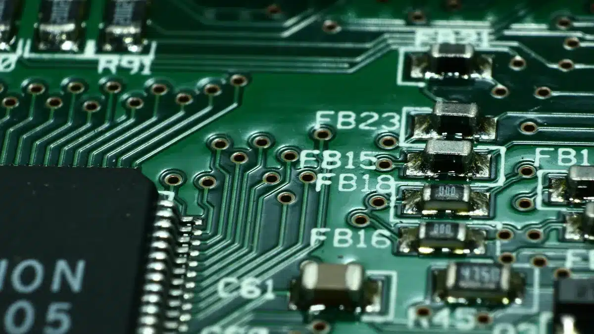
When you choose professional PCB layout services, your designs become much more accurate. Experts use special tools and methods to make sure every part of your PCB follows industry rules. Here are some important steps they take:
Process/Tool | Description |
|---|---|
Automatically checks that the design meets electrical and manufacturing rules. | |
Trace Routing | Makes sure traces are routed correctly to keep signals clear. |
Signal Integrity Analysis | Looks at electrical performance to reduce noise and interference. |
Component Placement | Arranges components to avoid problems and use space well. |
3D Visualization | Lets designers see layouts in 3D to spot possible issues. |
Auto-Routing and Interactive Routing | Automates trace routing but allows manual changes for better accuracy. |
Simulation and Testing | Tests how circuits perform virtually to find issues before making physical prototypes. |
By following these steps, professional services make sure your PCB layout works well and is trustworthy. This careful work lowers the chance of expensive mistakes during production. It helps you launch your product with confidence.
Time Efficiency
Time is very important in product development. Professional PCB layout services make the design process faster. This helps you meet tight deadlines without losing quality. Here are some tools and technologies that help save time:
Tool/Technology | Purpose |
|---|---|
Design Rule Checks (DRC) | Finds errors like overlapping traces and checks for manufacturing standards. |
Tests performance for hot spots and signal clarity before production. | |
Advanced PCB Design Software | Offers schematic capture, component libraries, and routing features to make design easier. |
Component Libraries and Footprint Generators | Ensure correct component placement and cut down on mistakes during design. |
These tools help designers work faster, cutting down on time spent fixing mistakes. This way, you can focus on other important parts of your project, like marketing and distribution.
Comparing PCB Layout Services to DIY
Cost Considerations
When you think about the costs of PCB layout, you might believe DIY methods save money. But, hidden costs can make DIY more expensive later. Here are some common problems you might face:
Signal Integrity Issues: Bad signal integrity can cause costly redesigns and delays. This is especially true for high-speed designs. Faulty products may reach customers, leading to recalls.
Thermal Management Problems: Not managing heat can cause components to overheat. This can lead to high return rates and warranty claims, hurting profits.
Even though professional PCB layout services may cost more at first, they often save you money by avoiding these hidden costs. You invest in quality and reliability, which leads to fewer mistakes and better performance.
Quality and Reliability
Quality and reliability are very important in PCB design. The difference between DIY methods and professional services can be huge. Look at this comparison:
Aspect | DIY Methods | Professional Services |
|---|---|---|
Precision and Accuracy | Limited trace width and manual placement issues | High precision with automated processes |
Reliability and Performance | Cold solder joints and inconsistent quality | Consistent solder joints and thorough testing |
Consistency and Repeatability | Variability in each PCB due to manual processes | Identical PCBs with quality control systems |
Good for low-frequency designs | Necessary for high-frequency and critical designs |
DIY PCB layouts often have reliability problems. Common issues include:
Reliability Issue | Description |
|---|---|
Signal Integrity | Problems like ground bounce, reflections, crosstalk, and ringing that can harm signal integrity. |
Ionic Contamination | Residues that become conductive in moisture, affecting reliability and function. |
Measling and Delamination | Circular white spots and holes that can disrupt PCB operations. |
Environmental Factors | Issues like dust, heat, and moisture that can cause overheating, corrosion, and rust. |
Electromagnetic Interference | Unwanted effects that can lead to defective products due to too much electromagnetic energy. |
By choosing professional PCB layout services, you make sure your designs meet high quality and reliability standards. This choice reduces risks and improves the overall performance of your products.
The PCB Layout Process

The PCB layout process has several important steps. These steps help make sure your design meets all the needed requirements. Each step is important for a good result.
Consultation and Requirements
The first part of the PCB layout process is consultation. In this stage, you collect important information to help with the design. Here are some key things to think about:
Decide where to place them on the PCB.
Identify critical signals that need special care.
Check power needs to make sure there is enough supply.
This first consultation helps you and the design team agree on project goals. It lays the groundwork for a successful layout by making expectations clear.
After gathering the needed information, the design team adjusts their approach to fit your needs. They look at important documents and confirm project details with you. This teamwork makes sure everyone understands before moving ahead.
Design and Simulation
Once the consultation is done, the design phase starts. This stage includes several key steps:
PCB schematic creation: Make a diagram showing the system’s components and how they connect.
Component placement: Arrange components based on how the circuit works.
Route the board nets: Lay copper traces to connect different points.
Perform a design rule check (DRC): Check that the design is logical and physically sound.
Complete PCB fab/assembly notes: Write down design information for manufacturing.
Each of these steps is very important for your project’s success. For example, setting the board outline early stops productivity loss from changes later. Good component placement reduces signal interference and heat issues.
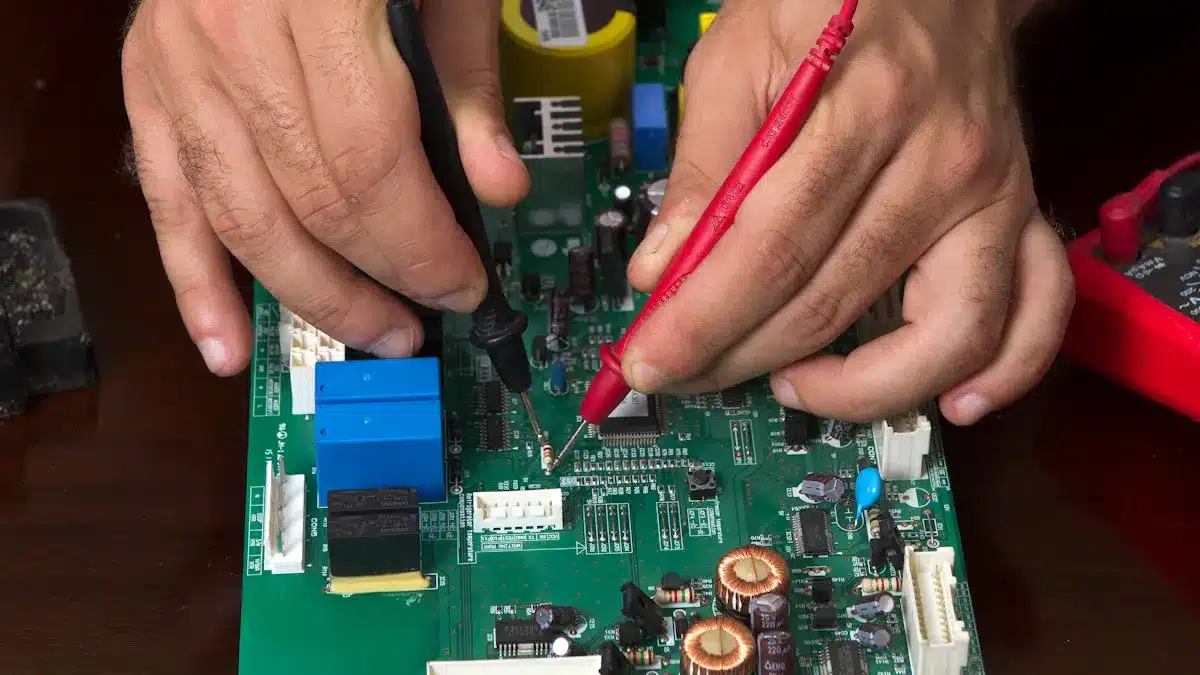
Simulation tools are very important for checking designs. Tools like ORCAD and Allegro PCB Designer help check signal quality and find problems before production. This careful approach lowers the chance of costly mistakes and makes sure your PCB layout meets high standards.
By carefully following these steps, you improve the reliability and performance of your PCB design. This helps lead to a successful product launch.
Case Studies in PCB Layout
Success Stories
Professional PCB layout services have helped many projects succeed in different industries. One important example is a product manufacturing company in the USA. This project cost $5,000 and used PADS software. The main benefits were a huge 40% cost savings, better teamwork, and access to expert knowledge. At first, the team had trouble understanding where to place parts and how to position connectors. In the end, they produced organized Gerber files for the client, making production easier.
Aspect | Details |
|---|---|
Client Profile | Product Manufacturing Company in the USA |
Project Cost | $5k / Project |
Software Used | PADS |
Key Benefits | 40% cost savings, improved coordination, and expertise access |
Initial Challenges | Understanding placement requirements and connector positions |
Final Output | Gerber files shared with the client |
Client Feedback
Clients often share their happiness with how professional PCB layout services help their projects. Here are some important points from their feedback:
Performance Optimization: Clients said that expert PCB layout helps with efficient signal routing and reduces electromagnetic interference, which is very important for high-speed applications.
Manufacturability: Feedback showed that designing for manufacturability lowers production costs and makes assembly easier, improving overall project efficiency.
Reliability and Compliance: Clients pointed out that good layouts lead to stronger boards and meet industry standards, which is crucial for mission-critical applications.
Client testimonials also show the value of these services. For example, Kevin said, “We have fully processed the complete run of your flexible circuit boards and had spectacular results. It is the only time we have had a 99% first pass yield for this particular board.” Other clients shared similar thoughts, praising timely deliveries and high-quality work.
Client Name | Testimonial |
|---|---|
Kevin | ‘We have fully processed the complete run of your flexible circuit boards and had spectacular results. It is the only time we have had a 99% first pass yield for this particular board.’ |
Andrew | ‘I really acknowledge the timely deliveries and the quality of work with your turnkey assembly services.’ |
Nitin Patel | ‘They have always been prompt in their deliveries and their quality has always remained top-notch.’ |
Raymond C | ‘Because of your quality, knowledge, and reliable execution, we didn’t have to worry about chips shortages.’ |
Luis Umbarila | ‘You got our complete batch of rigid-flex boards assembled in time. I really appreciate your customer focus.’ |
Nathan Burget | ‘The Assembly quality of all the boards has been excellent.’ |
Michael Eller | ‘We have received excellent quality of boards and quick turns, which is what keeps us coming back.’ |
Michael Jensen | ‘We greatly appreciate the quick response and turnaround you have done for us over the last couple of months.’ |
Davis Hoffman | ‘PCB Trace Technologies Inc. was punctual with the full turnkey services and made deliveries just in time.’ |
In summary, using professional PCB layout services has many benefits for your projects. You get expert help, modern tools, and careful testing that make your products more reliable.
Current trends show that the industry is moving towards using AI and IoT in PCB design. There is also a focus on being eco-friendly and following Industry 4.0 ideas. These changes will influence the future of PCB layout services and help you stay ahead of your competition.
By regularly using these services, you can make your design process smoother, lower costs, and boost product quality. This smart choice reduces design mistakes and speeds up your product development. It helps you launch new ideas to the market more quickly. 🌟
FAQ
What are PCB layout services?
PCB layout services are about designing printed circuit boards carefully. Experts use special software to make layouts that follow electrical and manufacturing rules. This ensures your product works well and is reliable.
How long does the PCB layout process take?
The time it takes for the PCB layout process can change based on how complex it is. Usually, it can take from a few days to several weeks. This depends on what the project needs and any changes made.
Can I make changes during the PCB design process?
Yes, you can change things during the PCB design process. Talking early helps find out what you need. This way, adjustments can be made as the design moves forward. Good communication with the design team is very important.
What industries benefit from PCB layout services?
Many industries gain from PCB layout services. These include consumer electronics, cars, medical devices, and telecommunications. Each area needs precise designs to make sure products are reliable and work well.
How do I choose a PCB layout service provider?
When picking a PCB layout service provider, think about their experience and skills. Check their past work and look for client reviews. Make sure they use advanced design tools to meet your needs.
See Also
Essential Guidelines for Choosing Top PCB Assembly Services
Key Factors in Choosing the Right PCBA Manufacturer
Steps to Identify the Ideal PCB Prototype Manufacturer