Additive manufacturing for PCBA in 2025 is changing electronics. This tech helps make complex PCBs with great accuracy. You can now build multi-layer boards and bendable circuits. These are perfect for new devices like 5G wearables. Better materials and methods allow more production with less waste. Additive manufacturing also works well with 5G tech for faster, stronger connections. These changes let you create prototypes quickly and design easily. It’s transforming how electronics are made.
Key Takeaways
Additive manufacturing helps make detailed, multi-layer PCBs with built-in parts.
This makes devices smaller and work better than before.
It speeds up testing, so designs improve in days, not weeks.
Faster testing helps companies stay ahead of their competition.
Using green materials cuts waste and saves energy during PCB making.
This helps both the planet and lowers business costs.
Flexible PCBs are key for modern wearables like smartwatches.
They are strong and allow cool designs in small spaces.
Teamwork between schools and companies improves additive manufacturing.
This leads to better materials and smarter ways to make things.
Overview of Additive Manufacturing in PCBA
What is Additive Manufacturing for PCBA?
Additive manufacturing, also called 3D printing, is changing PCBA. Instead of cutting material away, it builds PCBs in layers. This method allows for detailed designs that were once too hard to make. It also creates less waste, helping the environment. With this process, prototypes can be made faster and cheaper. These advantages make additive manufacturing a big step forward for PCB production.
How PCB Assembly Has Changed Over Time
PCB assembly has improved a lot since it started. At first, people made PCBs by hand, which was slow and had mistakes. Later, machines made the process faster and more accurate. But old methods still wasted materials and limited designs. Additive manufacturing brought a huge improvement. Now, complex PCBs can be made with less waste and more precision. This change has helped electronics grow and improve quickly.
Why Additive Manufacturing Matters in Electronics
Today, electronics need to be fast and customizable. Additive manufacturing helps by allowing quick prototypes and flexible designs. PCBs can now be made for special uses, like wearables or space tech. This method also adds advanced features, like built-in components. Using additive manufacturing keeps companies ahead in a tough market. It’s not just about making PCBs; it’s about creating new possibilities for electronics.
Key Breakthroughs in 2025
Multi-Layer PCB Production with Integrated Components
By 2025, making multi-layer PCBs has improved a lot. These changes let you design smaller and smarter boards. Components like resistors and microchips can now be built into the PCB layers. This means fewer extra parts are needed outside the board. The result is smaller, stronger designs for things like IoT gadgets and car systems.
Studies show multi-layer PCBs are key in many industries. Better materials and more layers make these boards last longer. For example:
Multi-layer PCBs are vital for cars and communication devices.
New methods improve how well built-in parts work.
Research proves these upgrades are useful and reliable.
These changes make PCBs work better and faster to build. Adding parts inside the board saves time and boosts reliability. This is a big step forward for making smarter, better devices.
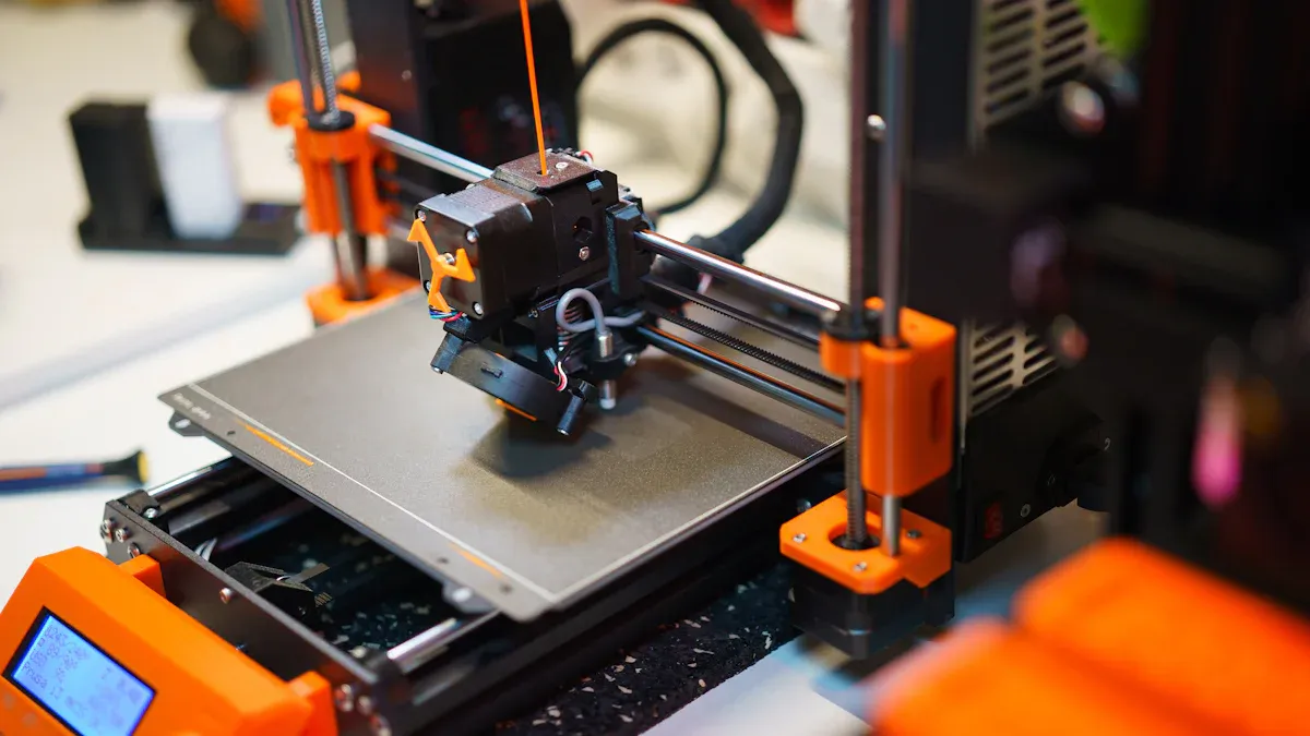
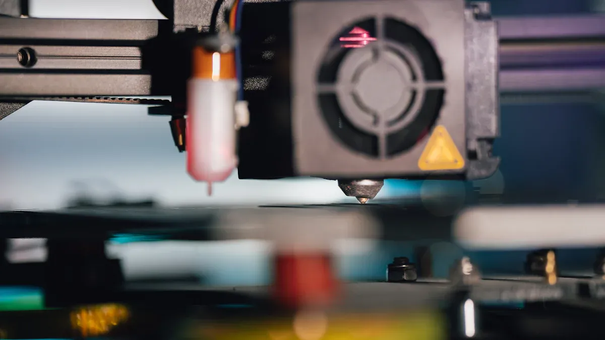
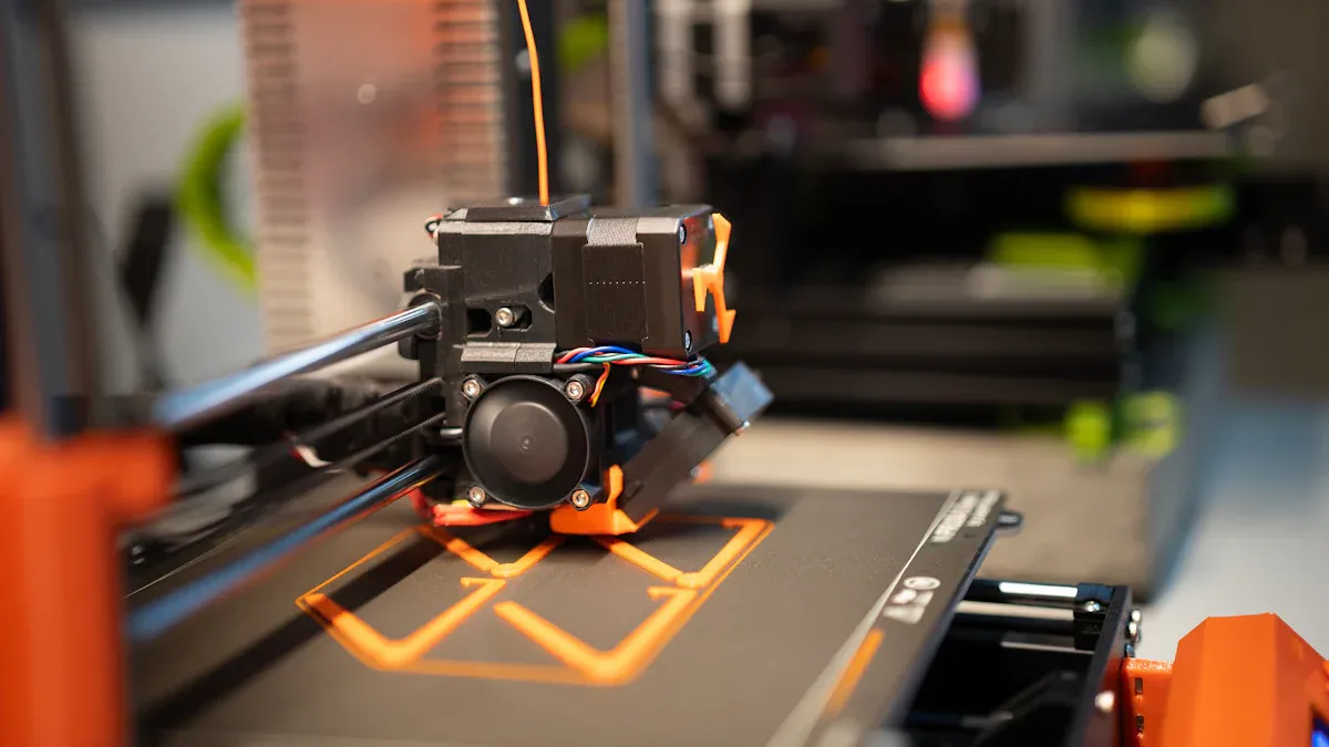
Advancements in 3D Printing in PCB Assembly
In 2025, 3D printing plays a bigger role in PCBs. This tech builds boards layer by layer, creating detailed designs. With 3D printing, you can add conductive and insulating materials in one go. This cuts waste and speeds up production, making it eco-friendly.
A big improvement is hybrid manufacturing. For example, mixing aerosol jet printing with nano-copper paste improves conductivity. This method creates circuits with very low resistance. New machines also combine processes like SLA and inkjet printing. These can make 10-layer PCBs in under two hours.
Reports show 3D printing is changing PCB assembly. For example:
Key Insights | Details |
|---|---|
Major Acquisitions | Nano Dimension’s deals boost the market. |
Revenue Growth | |
Industry Events | RAPID + TCT showed new 3D printing tech. |
3D printing helps make custom PCBs quickly and easily. Whether for testing or small batches, this tech offers great precision and flexibility.
Flexible PCBs for Wearable and Compact Devices
Flexible PCBs are now key for modern gadgets. These boards can bend and twist without breaking. They are perfect for fitness trackers, smartwatches, and medical devices. In 2025, better materials make flexible PCBs stronger and more useful.
New high-heat resins help these boards handle tough conditions. Techniques like laser structuring let you add antennas directly to the board. This keeps designs small but powerful.
Flexible PCBs are not just for wearables. Small devices in cars and planes also use them. They help make products lighter and smaller without losing performance. Flexible PCBs are crucial for building smarter, smaller electronics.
Sustainable Materials and Processes
Eco-friendly methods are changing how PCBs are made. Now, you can use green materials and save energy while reducing waste. These changes make PCB production cheaper and better for the planet.
Here’s why sustainable methods help manufacturers:
Attract eco-friendly buyers, making products more popular.
Get tax breaks for using green practices.
Boost worker happiness with teamwork on sustainability.
Cut pollution and help the environment.
New materials are key to greener circuit boards. Strong resins (Tg > 200°C) last through high-heat soldering. Mixing aerosol jet printing with nano-copper paste improves conductivity and lowers resistance. These upgrades make PCBs stronger and better for the Earth.
Using green processes helps the planet and your business. It’s a smart way to make products while protecting the future.
Benefits and Applications of These Advancements
Enhanced Design Flexibility and Customization
Additive manufacturing has changed how PCBs are made. It lets you create detailed designs and add parts directly to the board. This means PCBs can be made for specific uses, like small wearables or advanced car systems. Adding features like antennas or sensors inside the board reduces extra parts. This makes the assembly process simpler and faster.
For example, new methods like using copper layers or Laser Direct Structuring (LDS) antennas help balance performance and design. These ideas make PCBs more useful for new tech like IoT and AI devices. They allow engineers to create smarter and more flexible designs.
Tip: Using these new methods saves time and materials during production.
Accelerated Prototyping and Iteration Cycles
Additive manufacturing has made prototyping much faster. Old methods could take weeks or months to make a prototype. Now, designs can be created and tested in just days. This speed helps improve designs quickly based on real-world tests.
For example, a car parts supplier cut development time from months to weeks. This allowed them to test and improve designs faster. In healthcare, companies use rapid tools to make custom parts quickly. This helps them launch products faster than competitors using older methods.
Automation also helps speed up prototyping. Machines that make PCBs automatically are more accurate and efficient. They reduce mistakes and ensure prototypes are high quality and ready faster.
Cost-Effective Manufacturing for Low-Volume Production
Additive manufacturing is great for making small batches of PCBs. Traditional methods cost a lot to set up, which isn’t ideal for small runs. Additive techniques remove many of these costs, making it cheaper to produce high-quality PCBs.
Reports show more industries want affordable solutions, like in cars and telecom. The 3D electronics market is expected to grow to $4.3 billion by 2034. This shows more companies are using additive manufacturing for small, valuable projects.
Using eco-friendly materials and energy-saving methods can lower costs even more. This helps meet environmental rules and improves your business image. It also supports global efforts to protect the planet.
Note: Saving money with these methods lets you try new ideas and designs that were too expensive before.
Applications in IoT, Wearables, and Aerospace
Additive manufacturing is opening doors for IoT, wearables, and aerospace. These fields need small, efficient, and custom-made electronics. New manufacturing methods now make this possible with better accuracy and flexibility.
IoT: Smarter Devices, Faster Connections
The Internet of Things (IoT) connects many devices together. Additive manufacturing helps make PCBs with built-in antennas and sensors. This makes devices smaller and work better. For example:
Smart Homes: Devices like cameras and plugs use tiny PCBs for easy connections.
Industrial IoT: Factory sensors track machines and send data to improve work.
Did You Know? Multi-layer PCBs are key for IoT devices. Additive manufacturing makes them faster and cheaper to produce.
Wearables: Lightweight and Flexible Designs
Wearable gadgets need PCBs that are strong but can bend. Additive manufacturing creates flexible PCBs for small, curved spaces. This is great for fitness bands, smartwatches, and health devices.
Key improvements include:
Better Materials: Special resins and inks make flexible PCBs last longer.
Smaller Parts: Tiny components help make wearables sleeker and more comfy.
Wearables also benefit from quick prototyping. You can test designs fast to meet user needs before making more.
Aerospace: High Performance Under Extreme Conditions
Aerospace electronics must handle tough environments. Additive manufacturing makes PCBs that resist heat and are very strong. These are needed for satellites, planes, and space tools.
Uses in aerospace include:
Satellites: Light PCBs lower launch costs but stay reliable.
Avionics: Advanced PCBs help with navigation and safety systems.
Tip: Using eco-friendly materials in aerospace PCBs helps the planet and meets global goals.
Why These Applications Matter
Custom PCBs for specific industries give you an advantage. Whether for IoT, wearables, or aerospace, additive manufacturing helps you innovate. It saves time, cuts costs, and ensures top-quality products.
Conclusion: Additive manufacturing helps create smarter, smaller, and better electronics. This technology is shaping the future of IoT, wearables, and aerospace.
Challenges and Limitations
Standardization of Materials and Processes
Making PCBs with additive manufacturing has some challenges. One big issue is creating clear rules for materials and methods. Without these rules, it’s hard to make sure products work well. For example, the thickness of conductive layers must match power needs.
Groups like IPC and NIST are working to fix this. They are making guidelines to improve reliability and set limits for designs. Tools powered by AI also help. These tools predict problems like parts expanding differently when heated. This ensures designs meet industry standards.
Without clear rules, it’s harder to trust this technology. Setting strong guidelines will help more people use additive manufacturing confidently.
Reliability and Durability of Additive PCBs
Additive PCBs need to be tough and reliable. They must last in harsh conditions, but this is still a challenge. Traditional methods often make stronger products. For example, layers in additive PCBs need to bond tightly to meet standards.
Weather and movement can also cause problems. Tests that speed up aging help find weak spots in designs. These tests improve how long products last and how well they work.
Studies show reliability is a big concern. Fixing these issues is important for industries like aerospace and cars. Stronger designs will help additive PCBs gain trust in these fields.
Challenge/Limitations | Description |
|---|---|
Making 3D electronics quickly is still a problem. | |
Products need to be tough and dependable. | |
Market Acceptance | Many industries are slow to adopt this new technology. |
High Initial Investment Costs
Starting additive manufacturing for PCBs costs a lot of money. Machines and special materials are expensive. Small companies often can’t afford these costs.
You also need trained workers and custom-made inks, which add to expenses. Scaling up production for big projects is another challenge. High costs make it harder for this technology to grow quickly.
Buying advanced machines and materials is expensive for small businesses.
Hiring skilled workers and using special inks costs more money.
Making large amounts of products is difficult and costly.
Even though it’s pricey, additive manufacturing saves money over time. It reduces waste and speeds up production. Investing now can help companies stay ahead in the electronics industry.
Workforce Training and Skill Development
Making PCBs with additive manufacturing needs skilled workers. They must know how to use advanced machines and follow new methods. As this tech grows, training your team is key to staying ahead. It helps workers handle tough tasks and keep up with industry changes.
Why Training is Important
Workers need to learn the challenges of additive manufacturing. For example, they should know how to use special software for PCB designs. They also need to operate machines that print conductive materials. Without training, mistakes can happen, wasting time and materials.
Tip: Training programs help workers avoid errors and improve productivity.
Important Skills to Learn
Focus on these skills to prepare your team:
Machine Operation: Teach how to use 3D printers and hybrid systems.
Material Knowledge: Explain how conductive inks and eco-friendly resins work.
Quality Control: Train workers to check PCBs for problems and ensure quality.
Software Skills: Offer lessons on CAD tools and design software.
Ways to Train
Use these methods to teach your team:
Workshops: Hands-on practice with new tools and machines.
Online Courses: Learn anytime with flexible online lessons.
Mentorship Programs: Pair new workers with experienced ones to share tips.
Training Method | Benefits |
|---|---|
Workshops | Learn by doing with real tools |
Online Courses | Study anytime, anywhere |
Mentorship Programs | Share knowledge and build teamwork |
Long-Term Advantages
Trained workers make production faster and better. They also help your company create new ideas and stay competitive. Investing in training builds a strong team ready for additive manufacturing challenges.
Conclusion: Training your team is not just a cost; it’s a smart way to ensure your company’s future success.
Future Outlook and Industry Implications
Mass Adoption in Electronics Manufacturing
Additive manufacturing is set to change electronics production. This technology makes creating complex, custom parts easier. The market for additive manufacturing with metal powders will grow fast. It is expected to rise by 21.4% each year from 2023 to 2033. By 2033, the market may reach $3.99 billion. This growth shows the need for detailed designs in electronics, aerospace, and healthcare.
The global additive manufacturing market could pass $100 billion by 2032. This is six times higher than in 2022. Faster production systems are driving this increase. They cut costs and improve efficiency. More companies will likely use additive manufacturing for pcb production. Precision and customization are key reasons for this shift.
Year | Market Size (in billion USD) | CAGR (%) |
|---|---|---|
2024 | 19.34 | N/A |
2025 | 23.42 | 21.1 |
2029 | 50.49 | 21.2 |
Enabling Next-Generation Technologies
Additive manufacturing helps create future-ready products. It allows pcbs to include antennas, sensors, and other parts. This supports next-gen devices like IoT gadgets and wearables. Hybrid methods, such as adding copper layers or LDS antennas, improve designs. These techniques balance performance and flexibility.
New materials like high-heat resins and nano-copper paste are game-changers. They make products stronger and better at conducting electricity. Additive manufacturing speeds up prototyping and production. This gives companies an edge in a fast-changing market.
Collaboration Between Industry and Academia
Teamwork between companies and schools is vital for growth. Universities and research groups help develop new materials and methods. Groups like IPC and NIST set rules for reliable 3D-printed pcbs. These partnerships turn ideas into real-world solutions.
AI tools from these collaborations predict design risks, like heat expansion issues. This ensures products meet industry standards. Working together helps solve problems and unlock additive manufacturing’s full potential.
Tip: Follow industry-academia projects to stay ahead in additive manufacturing.
Predictions for Additive Manufacturing in the Next Decade
The next ten years will bring big changes to additive manufacturing for PCBA. Expect faster machines, more material choices, and better teamwork with older methods. These updates will help meet the need for custom, high-quality electronics.
Key Innovations to Watch
Experts believe these breakthroughs will shape the future:
Printing Speed: Machines will make PCBs quicker, cutting production time a lot.
Material Diversity: New materials, including eco-friendly ones, will allow creative designs.
Mass Production: Additive methods will handle large orders while staying precise.
High Consistency: Improved systems will ensure every piece meets strict quality rules.
Seamless Integration: Additive tools will work smoothly with current systems, saving time.
Did You Know? By 2035, additive manufacturing might lower costs by 30% and boost sustainability.
Emerging Trends in Technology
New tech will also make additive manufacturing even better:
AI Integration: Artificial intelligence will improve designs and catch problems early.
Bioprinting: Though new, bioprinting could change how medical devices are made.
Sustainability: Green materials and energy-saving methods will make production cleaner.
These improvements will change how PCBs are built and create new uses in fields like healthcare, aerospace, and IoT. As additive manufacturing grows, it will keep pushing the limits of what’s possible in electronics.
Tip: Keep up with these trends to stay ahead in the fast-changing manufacturing world.
The progress in additive manufacturing for PCBA in 2025 is changing how electronics are made. This method allows detailed designs, quicker prototypes, and making parts when needed. Multi-layer PCBs with built-in components are now possible. These improve how devices work while making them smaller. Using eco-friendly materials and mixed techniques also helps protect the planet.
Key Takeaway: Additive manufacturing uses AI, smart machines, and new ideas to make better, greener electronics. Keeping up with this technology and working together will help you stay ahead in this fast-changing field.
FAQ
What is additive manufacturing, and how is it different?
Additive manufacturing builds PCBs layer by layer. Traditional methods cut material away. This process wastes less and allows complex designs. It also makes production faster and lets you customize easily. It’s great for modern electronics like IoT devices and wearables.
Can additive manufacturing make flexible PCBs?
Yes, it can! Flexible PCBs use special materials that bend but don’t break. These boards are ideal for wearables, medical tools, and small gadgets. Additive manufacturing keeps them strong while making them flexible for creative designs.
Is additive manufacturing good for the environment?
Definitely! Additive manufacturing uses eco-friendly materials and creates less waste. It also uses less energy than older methods. Green practices save money, follow environmental rules, and help protect the planet. 🌱
Which industries benefit most from additive manufacturing?
Industries like IoT, aerospace, and wearables benefit the most. IoT devices need small, multi-layer PCBs. Aerospace needs strong, lightweight boards. Wearables need flexible, tiny designs. Additive manufacturing delivers these with speed and accuracy.
How can you start using additive manufacturing?
Start by buying 3D printers and training your team. Learn about materials like nano-copper paste and heat-resistant resins. Work with experts or join workshops to understand the process. Begin small and grow as you learn more.
Tip: Team up with industry leaders to learn faster.
See Also
Emerging Innovations in PCB and PCBA Design Techniques
Benefits and Hurdles of Flex PCBA in Electronics Today
Essential Strategies for Overcoming PCBA Manufacturing Obstacles
The Importance of Custom PCBA Production in Today’s Electronics
Choosing PCBA Manufacturing Services with Cutting-Edge Features