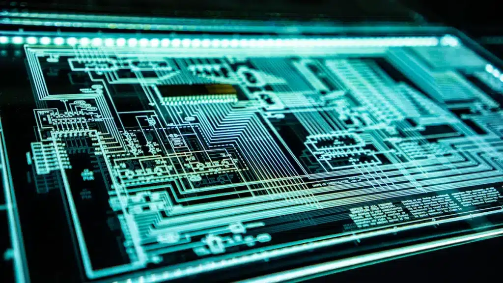
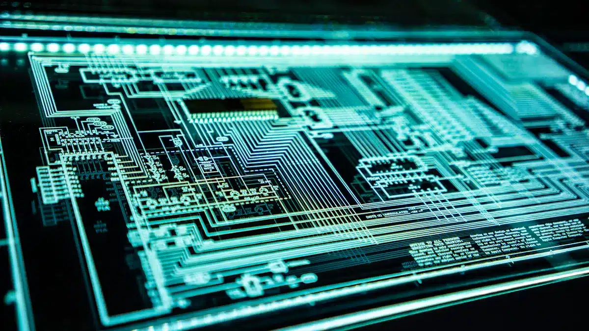
The move to 3D printed circuit boards shows a big change in technology. You can quickly change designs and make prototypes. This flexibility helps you create special shapes just for you. Also, 3D printing can handle complex designs that old methods can’t. As you look into this new way, you’ll see it cuts down costs and waste. This makes it a great choice for today’s electronics.
Key Takeaways
3D printed circuit boards help save money. They do this by using less material and needing less work. This makes them great for small orders and prototypes.
This technology lets designers change things quickly. It can also create complex shapes. This helps speed up product development and new ideas.
3D printing makes production much faster. Prototypes can be made in hours, not days or weeks.
Using 3D printed circuit boards is good for the environment. They create less waste and use fewer harmful chemicals.
3D printed PCBs have better performance features. They can resist higher levels and manage heat better. This makes them good for many uses.
Cost Savings
3D printed circuit boards save a lot of money compared to old ways of making them. One big benefit is less wasted material. Traditional PCB making often cuts away extra material, which creates a lot of waste. But 3D printing only uses the material needed for the design. This smart use of materials lowers costs and helps the environment.
A study from Beta LAYOUT shows these savings. They switched to additive manufacturing for circuit carriers. This change got rid of expensive injection molding. It also allowed them to make products without tools, which cut costs a lot. They could create complex, multi-layer circuit designs that old methods find hard to make.
For small orders and prototypes, 3D printing is great. Old methods often need costly setups and tools, making small runs hard to do. With 3D printing, you can make just a few units without high costs. This is especially helpful for startups and small businesses that want to test ideas without spending too much.
CircuitHub’s case studies show that companies like Formlabs and Blue Robotics have made their prototyping faster by using digital manufacturing platforms. These platforms make production easier and cut down on material waste, leading to more savings.
Another thing to think about is labor costs. The table below shows labor costs for traditional PCB production and 3D printed circuit boards:
Cost Factor | Traditional PCB | 3D Inkjet PCB |
|---|---|---|
Labor/Unit | $0.25 |
As you can see, labor costs for 3D printed circuit boards are much lower. This drop in costs helps save money overall, making 3D printing a good choice for many businesses.
Design Options
3D printing gives you great choices in PCB design. You can make detailed shapes and layouts that old methods can’t do. This technology lets you try different designs without the limits of traditional manufacturing. Here are some main benefits of using 3D printing for your circuit boards:
Rapid Design Iteration: You can test designs in just hours. Old methods often take weeks to make. This quick testing helps you develop products faster and improve your ideas quickly.
Complex Geometries: 3D printing lets you create complicated shapes and non-flat designs. For instance, you can make rigid-flex PCBs that join several rigid boards with flexible materials. This ability allows for special interconnect vias and placing parts on non-flat surfaces.
Increased Packing Density: With 3D printed circuit boards, you can fit more parts in a smaller area. This is important for compact designs, especially where space is tight.
Reduced Weight: The design freedom of 3D printing leads to lighter assemblies. This weight reduction is important in many areas, like aerospace and portable electronics.
Integration of Components: You can connect circuit parts directly, which removes the need for connectors and cables. This makes the design simpler and improves reliability.
The table below shows the benefits of 3D printing compared to traditional methods:
Advantage | 3D Printing | Traditional Methods |
|---|---|---|
Allows complex geometries and customization | Limited to flat designs and manual assembly | |
Material Waste | Minimal waste due to additive process | Significant waste from subtractive methods |
Production Speed | Rapid prototyping and iterations | Time-consuming with multiple steps |
Cost Efficiency | Lower labor and material costs | Higher costs due to skilled labor and setup |
Design Complexity | Supports intricate designs | Limited by manual soldering capabilities |
Speed of Production
3D printing makes making circuit boards much faster. You can create prototypes in a short time compared to old methods. Here are some important points to think about:
Rapid Prototyping: With 3D printed circuit boards, you can make prototypes in less than 24 hours. Traditional PCB prototyping usually takes about 8 days. For complex, multi-layer boards, 3D printing can finish in just 2-4 hours. Old methods often take days or even weeks.
Time-to-Market Benefits: Faster production means new electronic products can hit the market sooner. You can prototype designs at your place, making it easy to change and improve them. For example, PHYTEC added a new 3D printer to their process. This change led to shorter production times and quicker market entry. Now, making a PCB prototype takes only 12-18 hours, showing a big difference in time-to-market.
Overall Efficiency: The quick prototyping of 3D printed circuit boards helps research and development teams. They can test and check designs fast, speeding up the whole development process. Here’s a summary of the benefits:
Benefit | Description |
|---|---|
Speed | Cuts down the time to make a PCB prototype from days or weeks to just hours. |
Cost-Effectiveness | Removes high setup costs linked to traditional PCB making, making it cheaper. |
Flexibility | Allows quick design changes and updates without needing new tools or setups. |
Complexity | Lets you create complicated, multi-layer circuits with built-in parts. |
Accessibility | Low-cost 3D printers and materials make PCBs easier for more designers and engineers to use. |
By choosing 3D printed circuit boards, you save time and improve your ability to create and meet market needs quickly.
Environmental Benefits
3D printed circuit boards have many good effects on the environment compared to traditional PCB making. One big advantage is that they use fewer resources. Studies show that 3D printing works better for the environment than old methods. For example, different 3D printing ways show great cuts in environmental harm:
Direct Ink Writing (DIW): 23.95%
Inkjet Printing (IJP): 14.29%
Aerosol Jet Printing (AJP): 32.98%
These numbers show how 3D printing makes less waste and saves resources.
Another important point is that it uses fewer harmful chemicals. Traditional PCB making often uses toxic materials that can hurt the environment. But 3D printed circuit boards cut down or get rid of these chemicals. The table below shows some harmful chemicals in 3D printed PCB making:
Hazardous Chemical | Status in 3D Printed PCB Manufacturing |
|---|---|
Formaldehyde | Eliminated |
EDTA | Reduced |
Other hazardous substances | Reduced |
This drop in harmful chemicals makes 3D printing a safer choice for nature.
Also, 3D printed circuit boards help with better ways to dispose of them when they are done. They help lower electronic waste (e-waste) in landfills, which supports a circular economy. Here are some benefits of 3D printed PCBs for disposal:
Reduced E-Waste: Compostable PCBs help cut down e-waste in landfills.
Lower Toxicity: Biodegradable PCBs do not have harmful chemicals, making disposal safer.
Energy Efficiency: Throwing away biodegradable PCBs usually takes less energy than recycling old boards.
Performance of 3D Printed Circuit Boards
3D printed circuit boards have great performance benefits compared to old methods. You will see better electrical features that make them good for many uses. For example, 3D printed PCBs can have resistance levels that are 10 to 100 times higher than copper. This means they can carry more current without getting too hot. But, they might not work well in high-frequency situations. They usually do well up to 100 MHz, while regular PCBs work better in high-frequency areas.
Thermal management is another important area where 3D printed circuit boards do well. They often use materials that can handle moderate heat. However, they might not deal with extreme heat as well as traditional PCBs, which can take temperatures up to 130°C. Here’s a quick look at the performance differences:
Aspect | 3D Printed PCBs | Conventional PCBs (FR-4) |
|---|---|---|
Resistance | 10-100 times higher than copper | Lower resistance (copper) |
High-Frequency Limit | Affected above 100 MHz | Better performance at high frequencies |
Thermal Stability | May not withstand high temperatures | Can withstand up to 130°C |
In conclusion, 3D printed circuit boards have many benefits compared to old methods. You get faster production times, lower material costs, and more design options. Experts say that 3D printing reduces mistakes and waste, making it a great choice for the future.
Here are some key trends:
Advanced Materials: Research is looking at new conductive inks for better performance.
Integration with IoT: Smart parts can cut maintenance costs by up to 25%.
Hybrid Manufacturing: Mixing 3D printing with traditional methods makes things more efficient.
Since the market for 3D printed circuit boards is expected to grow a lot, now is the best time to check out this cool technology. 🌟
FAQ
What are 3D printed circuit boards?
3D printed circuit boards (PCBs) are electronic circuits made with 3D printing. This way lets you create complex designs and makes production faster than old methods.
How do 3D printed PCBs save costs?
3D printed PCBs cut down on material waste and labor costs. You can make small batches without needing expensive setups. This makes them great for prototypes and small orders.
Are 3D printed circuit boards reliable?
Yes, 3D printed circuit boards can be reliable. They have better electrical features and improved heat management. This makes them good for many uses.
Can I use 3D printed PCBs for high-frequency applications?
3D printed PCBs work well up to 100 MHz. For high-frequency uses, traditional PCBs might work better because they perform well in those ranges.
What materials are used in 3D printed PCBs?
3D printed PCBs use different materials, like conductive inks and thermoplastics. These materials give flexibility and strength while allowing for creative designs.
See Also
Exploring The Benefits And Challenges Of Flex PCBA
The Importance Of Custom PCBA Manufacturing In Electronics
Essential Factors To Evaluate When Selecting PCB Or PCBA