You use devices with circuit boards every day, such as phones and cars. Circuit board manufacturing transforms simple materials into advanced electronics on a massive scale. In 2024, over 87.4 billion square inches of printed circuit boards were produced, with the Asia-Pacific region leading in production. To ensure a high-quality board, the circuit board manufacturing process includes several key steps:
Design and layout
Fabrication
Assembly
Testing
Each step is essential to making sure the board functions properly and meets quality standards.
Key Takeaways
Circuit board manufacturing has four main steps. These are design, fabrication, assembly, and testing. Each step helps make sure the board works well and is good quality.
Design begins with making a schematic using software. The schematic is changed into files for the factory. This helps stop mistakes and saves time.
Materials like substrates, copper, solder mask, and silkscreen are important. Each material helps the board stay strong, resist heat, and stay safe.
Manufacturing uses steps like printing patterns and etching copper. It also includes drilling holes, layering, plating, and grouping boards. These steps help make more boards faster.
Testing and inspection find problems early. Tools like AOI and X-rays are used. This makes sure boards work well before assembly and shipping.
Design
Schematic Creation
The first step is to make a schematic. This is a picture that shows how parts connect. You use special software to draw it. Some popular programs are Altium Designer, Autodesk EAGLE, KiCad, and OrCAD. These tools help you plan and find mistakes before you go on.
Here is a table that lists the main features of these design tools:
Software Name | Key Features | Typical Users | Platform Compatibility |
|---|---|---|---|
Altium Designer | Advanced design, 3D visualization, DFM tools | Professionals, industries | Windows |
KiCad | Free, open-source, 3D viewer | Beginners, students, small firms | Linux, Windows, macOS |
Autodesk EAGLE | Large library, Fusion 360 integration | Hobbyists, small businesses | Mac OS X, Linux |
OrCAD | Simulation, advanced PCB features | Professional engineers | Not specified |
You pick your software based on what you need. If you want more features, you might use Altium Designer. If you are new, KiCad is a good pick because it is free and simple.
Design Conversion
When your schematic is done, you must turn it into files for the factory. This step is very important. The design software changes your diagram into files like Gerber files and drill files. These files tell the machines how to make your board.
Tip: Always do design rule checks (DRC) and electrical rule checks (ERC) before you send files to the factory. These checks help you find mistakes early.
Making these files gives a clear plan for the whole job. This helps stop problems like signal issues or short circuits. Your software also helps you put parts in place and draw the paths. Automated tools make this step quick and correct.
You also add a Bill of Materials (BOM) with your files. This list tells the factory which parts to use. Good design conversion saves time, lowers mistakes, and helps your board work right.
Materials
Substrate
The substrate is the base of your circuit board. It gives the board its shape and strength. It also keeps electricity from leaking. Different projects need different substrates. Here are some common types:
Ceramic substrates like alumina and aluminum nitride can handle high heat. They also insulate well. You find them in power electronics, cars, and planes.
Flexible substrates such as polyimide and PTFE (Teflon) can bend and resist heat. These are good for wearables and sensors.
Metal core substrates use aluminum or copper to move heat away from hot parts. LED lights often use these.
Rigid PCBs use hard materials to stay strong. They are great for computer motherboards.
Rigid-flex PCBs mix hard and bendy layers. This saves space in medical and military devices.
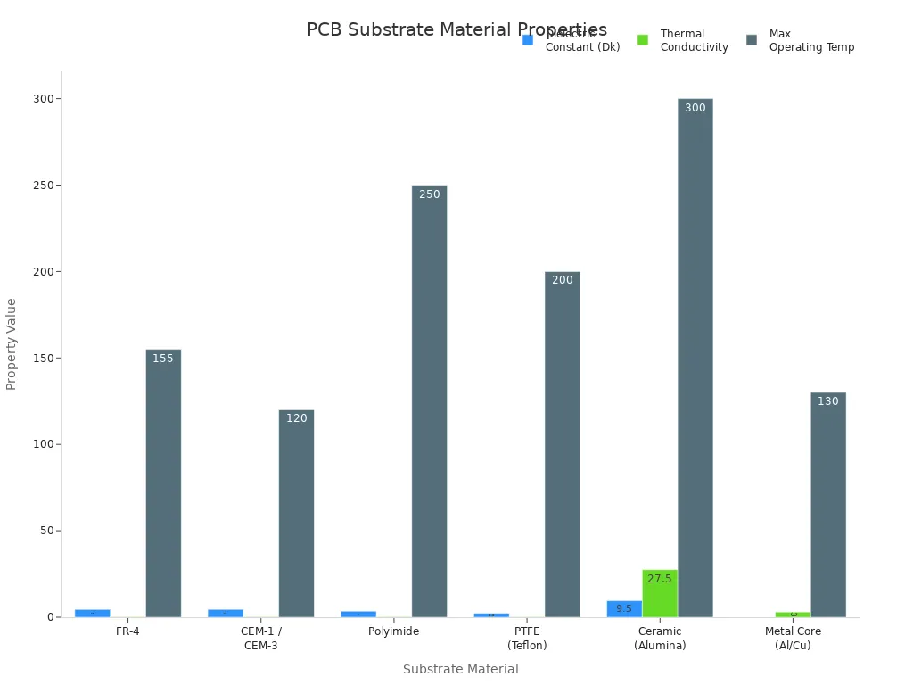
Here is a table that shows the properties of popular substrate materials:
Substrate Material | Dielectric Constant (Dk) | Thermal Conductivity (W/m·K) | Max Operating Temp (°C) | Typical Applications |
|---|---|---|---|---|
FR-4 | 4.2–4.8 | 0.3 | 130–180 | Consumer electronics, industrial devices |
CEM-1 / CEM-3 | ~4.5 | 0.25–0.3 | 110–130 | Low-cost single/double-sided PCBs |
Polyimide | ~3.5 | 0.2–0.3 | >250 | Flexible PCBs, aerospace, medical electronics |
PTFE (Teflon) | 2.1–2.5 | 0.25 | >200 | RF, microwave, radar communication |
Ceramic (Alumina) | 9–10 | 20–35 | >300 | Power electronics, automotive, aerospace |
Metal Core (Aluminum/Cu) | Varies | 1–5 | >130 | LEDs, high-current boards |
Copper
Copper makes the paths for electricity on your board. There are two main types: Electrolytic (ED) copper and Rolled Annealed (RA) copper. ED copper is good for inside layers and is smooth. RA copper bends well and sticks to the surface.
Copper thickness is measured in ounces per square foot. One ounce is about 1.4 mils thick.
Most boards use 1 oz copper. Some use 0.5 oz, 2 oz, or even thicker for special jobs.
The copper is very pure—about 99.7%. This helps signals move without loss.
Tip: Thicker copper can carry more current. But it costs more and takes longer to make.
Solder Mask
The solder mask covers the copper lines on your board. It keeps solder in the right spots. It stops bridges and shorts. It also protects against rust and keeps the board neat.
Solder mask is a thin, non-conductive plastic layer. It is usually about 20 microns thick.
It covers the lines, shows where parts go, and blocks water and dirt.
Common materials are epoxy (for most uses), polyimide (for high heat), and acrylic (for special needs).
You can pick from Epoxy Liquid, Liquid Photoimageable (LPI), and Dry Film Solder Mask.
Note: The solder mask also helps machines put parts in the right place during assembly.
Silkscreen
The silkscreen layer prints labels, logos, and part numbers on your board. It uses a strong, non-conductive ink. Makers use UV photo-imaging or direct printing for small details.
White is the most common color. It stands out on green, blue, or black solder masks.
Black is good for lighter boards.
Yellow is rare but helps when you need more contrast.
The silkscreen helps you find parts and connections fast. This makes assembly and repair much easier.
Circuit Board Manufacturing
Circuit board manufacturing turns your design into a real, working board. This process uses many steps to make sure your board is strong, accurate, and ready for assembly. Each step builds on the last, so you get a board that works well in your device.
Printing
Printing is the first step where your design becomes real. You start by sending Gerber files to the factory. These files tell the machines where to put copper and where to leave it off. The factory uses special printers to make photo films that show the pattern of your circuit.
You have three main ways to print the pattern onto the copper board:
Photolithography: You cover the board with a light-sensitive layer called photoresist. Then, you shine UV light through a mask with your circuit pattern. The light hardens the photoresist in the right places.
Screen Printing: You use a stencil to put ink on the board. The ink protects the copper you want to keep.
Direct Imaging: A laser or inkjet printer draws the pattern right onto the board. This method is fast and does not need a mask.
After printing, the board shows the exact paths for electricity. This step is key in circuit board manufacturing because it sets the stage for all the next steps.
Tip: Direct imaging is great for complex or small patterns because it gives high accuracy.
Etching
Etching removes the extra copper from your board. Only the copper covered by the hardened photoresist or ink stays. The rest gets washed away by chemicals.
Common etching chemicals include:
Ferric chloride
Copper chloride
Sodium persulfate
Ammonium persulfate
The choice of chemical and how you control it affects the quality of your board. You want sharp lines and no extra copper left behind. You also need to watch the temperature and how strong the chemicals are. If you do not control these, you can get rough edges or even damage the board.
Here is a simple list of the etching steps:
Clean the board to remove dirt.
Apply photoresist to protect the copper you want.
Dip the board in the etching solution.
Agitate the solution to make etching even.
Remove the photoresist and clean the board.
Note: Good etching means your board will have clean, sharp lines that match your design.
Drilling
Drilling makes holes for parts and connections. You use CNC drilling machines for most boards. These machines follow your design files and drill each hole in the right spot. They can hit an accuracy of about ±0.05 mm. For very small holes, like in high-density boards, you use laser drilling.
CNC drilling machines (for most jobs)
Laser drilling systems (for tiny holes)
Automated drilling systems (for big batches)
Drilling must be very precise. If the holes are off, your parts will not fit or connect right. CNC machines use hard drill bits and can spin very fast, up to 100,000 RPM. Laser drilling does not touch the board, so it works well for thin or delicate layers.
Tip: Clean, accurate holes help your board work better and last longer.
Lamination
Lamination bonds all the layers of your board together. If you have a simple board, you might only have one or two layers. Many modern boards have four, six, or even more layers. Each layer must line up perfectly.
You use registration holes and alignment tools to stack the layers. For a 4-layer board, you use at least three holes. For more layers, you use five or more. Sometimes, you use rivets or solder joints to hold the layers in place before pressing them together.
The layers go into a press that uses heat and pressure. This fuses them into one solid board. After lamination, you check the alignment with optical tools like X-ray or Automated Optical Inspection (AOI). This step makes sure the layers did not shift.
Note: Good alignment during lamination prevents shorts and open circuits in your finished board.
Plating
Plating covers the drilled holes with copper. This step lets electricity flow from one layer to another. You use a chemical process called electroless copper plating. The copper coats the inside of each hole, making a strong connection.
The typical copper thickness inside the holes is 20 to 30 microns. This is about as thick as a human hair. You measure the thickness with special tools to make sure it meets the standard. If the plating is too thin, the board can fail. If it is too thick, parts might not fit.
Sometimes, you use advanced methods like pulse plating or ultrasonic agitation. These help the copper spread evenly, even in deep or narrow holes.
Tip: Proper plating gives your board both strength and good electrical flow.
Panelization
Panelization groups many boards together on one large panel. This step makes circuit board manufacturing faster and cheaper. You can move, test, and assemble many boards at once. This saves time and lowers costs.
Benefits of panelization:
Speeds up production and lowers labor costs
Improves quality by reducing damage during handling
Makes it easier to use automated machines
You must plan the panel layout carefully. If you do not, you can waste material or make it hard to cut the boards apart later. Good panelization can cut assembly time in half and save up to 20% on materials.
Note: Panelization is a smart way to boost efficiency in circuit board manufacturing, especially for large orders.
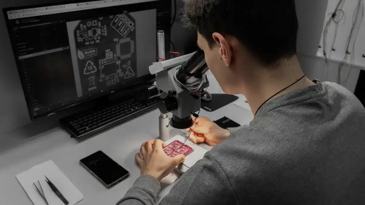
Testing
Testing checks if your circuit board works right. It also makes sure it meets quality rules. You use different ways to find and fix problems before putting parts on.
AOI
Automated Optical Inspection, or AOI, uses cameras and computer programs. These tools look for mistakes on your board. AOI helps you find errors fast and stops people from missing things. You can use AOI after solder paste, before and after reflow, and during wave soldering.
AOI can find many types of problems:
Parts put in the wrong spot, turned, or missing
Soldering issues like too little or too much solder, solder bridges, lifted leads, and tombstoning
Shorts and open spots
Wrong or upside-down parts
Scratches or bumps on the surface
Dirt or other things on the board
AOI looks at pictures of your board and compares them to a perfect board or CAD data. This makes checking faster and more correct. AOI can also sort problems and track boards by reading barcodes.
Tip: AOI lets you find and fix problems early. This saves you time and money.
Electrical Testing
Electrical testing checks if your board works the way it should. You use different tests to find problems:
Solderability testing checks if solder joints are strong and not rusty.
Contamination testing finds chemicals that can cause rust.
Micro-sectioning cuts and polishes a piece to look for shorts, opens, or bad solder.
Automated X-ray Inspection, or AXI, finds hidden problems like empty spots, shorts, or BGA issues.
Looking at the board with a microscope helps you see small soldering and assembly problems.
You also test how strong your board is by putting it through shaking, heat, power, and chemical tests. These tests follow rules like IPC and MIL-STD.
Note: Electrical testing helps you find things that could make your board break when used.
Final Inspection
Final inspection checks if your board is ready to be built and shipped. You follow these steps:
Automated Solder Paste Inspection, or SPI, checks if the solder paste is the right amount and in the right place.
First Article Manual Inspection makes sure parts match the list and are in the right spot.
AOI checks each board against a perfect one for mistakes and bad solder.
X-ray Examination finds hidden solder problems, especially for BGAs.
Endoscopic Inspection lets you see solder joints around the edges of BGAs.
Incoming Component and Material Inspection checks if parts are good before building.
Final Quality Inspection looks for soldering problems, parts in the wrong place, and electrical faults.
You use all these steps to make sure every board is good before it leaves the factory.
Assembly
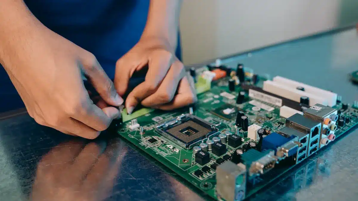
Component Placement
You start assembly by placing components on your circuit board. You can use two main methods:
Surface Mount Technology (SMT): Machines place small parts directly on the board. This method uses solder paste and pick-and-place robots. SMT lets you fit more parts in less space and speeds up production.
Through-Hole Technology (THT): You insert parts with wire leads into drilled holes. Workers or machines then solder these leads. THT gives strong connections and works well for parts that handle lots of power.
When you place components, follow these steps for best results:
Add main chips and power parts next.
Put smaller parts like resistors and capacitors last.
Group parts by function—keep power, analog, and digital parts apart.
Leave enough space between parts to avoid heat and noise problems.
Tip: Automated machines use cameras to check that each part sits in the right spot.
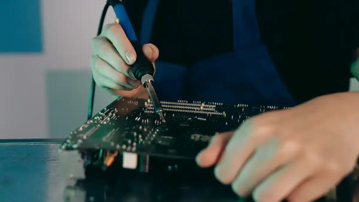
Soldering
Soldering joins your parts to the board. You can use several methods. Here is a table that shows the main types:
Soldering Technique | Description | Advantages |
|---|---|---|
Reflow Soldering | Heats solder paste to melt and bond SMT parts | Precise, automated, best for SMT |
Wave Soldering | Runs board over a wave of molten solder for THT parts | Fast, cost-effective, strong joints |
Hand Soldering | Uses a soldering iron for small jobs or repairs | Flexible, good for prototypes |
Selective Soldering | Targets certain areas for mixed SMT and THT boards | Precise, less heat damage |
Profiling
You must control heat during soldering. Thermal profiling helps you do this. You attach sensors to your board and run it through the oven. The sensors track temperature at key spots. You then adjust oven settings to make sure solder melts just right. This step stops defects like cold joints or damaged parts.
Note: Good profiling means every joint is strong and reliable.
Packaging
After assembly, you need to protect your boards. Use antistatic bags to stop static electricity. Add bubble wrap or foam to cushion against bumps. For boards that fear moisture, seal them in vacuum bags with desiccant packets. Always label packages with ESD warnings.
Shipping
You can ship boards in several ways:
Courier services like FedEx or DHL deliver small to medium packages fast and safely.
Freight shipping works best for large orders but takes longer.
Postal services cost less for small shipments but move slower.
Always use strong packaging and tracking to keep your boards safe and on time.
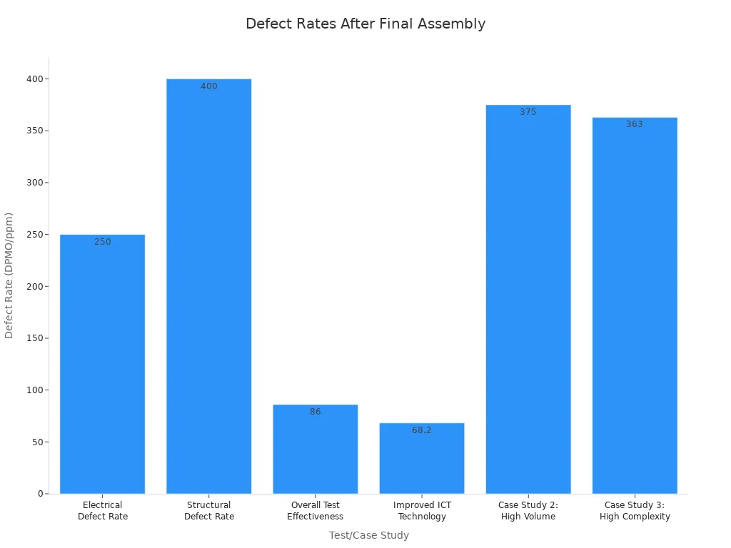
You help make circuit boards by knowing each step. Each stage is important for making boards work well. Quality checks like solder paste inspection, AOI, X-ray, and functional testing find problems early. These checks help keep the number of bad boards low.
Solder Paste Inspection stops weak joints from happening. 2. AOI looks for parts that are not in the right place. 3. X-ray lets you see hidden connections inside the board. 4. Functional Testing makes sure the board works in real life.
Today’s boards are harder to make than before. When you look at a finished PCB, think about the careful work and teamwork it took.
FAQ
What is the most common material for circuit board substrates?
You will find FR-4 as the most popular substrate. FR-4 is a fiberglass-reinforced epoxy laminate. It gives your board strength and good insulation. You can use it for most consumer electronics.
How do you choose between SMT and THT assembly?
You should use SMT for small, lightweight parts and high-density boards. THT works best for large or heavy parts that need strong connections. You can mix both methods for complex boards.
Why do you need a solder mask on a PCB?
The solder mask protects copper traces from short circuits and corrosion. It also keeps solder in the right places during assembly. You get a cleaner and more reliable board with a solder mask.
Can you repair a circuit board if it fails testing?
Yes, you can repair many boards. You might replace damaged parts, fix broken traces, or resolder joints. Some boards with severe damage may need replacement instead.
See Also
Exploring The SMT Process In PCBA Assembly Workflows
Key Steps Involved In The PCBA Manufacturing Process
A Clear Overview Of PCBA Manufacturing And Assembly