Printed circuit boards (PCBs) are very important in today’s electronics. They are the main part of many devices. You depend on PCBs to make things work, like smartphones and medical devices. Understanding the pcb manufacturing steps can be hard to grasp. Knowing this step-by-step guide to pcb manufacturing steps is important for good quality and efficiency. Complicated designs can raise production costs and take more time. So, understanding each detail of the pcb manufacturing steps helps you manage the manufacturing process better.
Key Takeaways
PCBs have three main types: rigid, flexible, and rigid-flex. Each type is good for different uses and designs.
Making a PCB involves design, picking materials, imaging, etching, drilling, plating, and finishing steps.
Quality assurance checks for problems early. This helps make sure PCBs work well.
Following industry rules and picking the right materials helps PCBs perform better and last longer.
Final testing makes sure the PCB works well before it goes to customers. This ensures high quality and reliability.
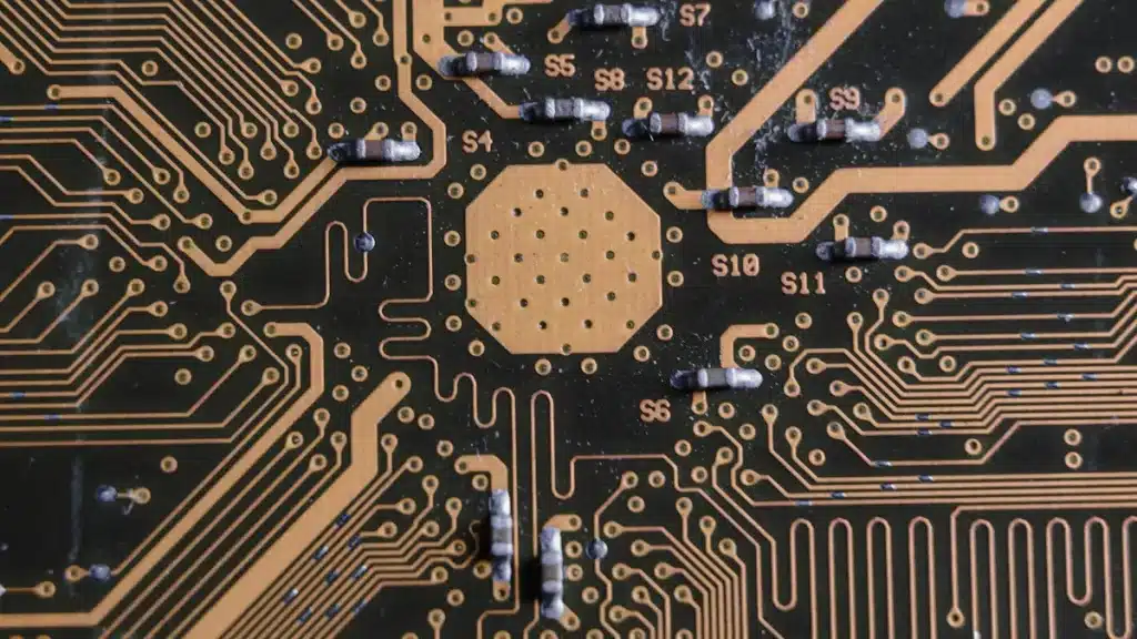
PCB Types and Importance
Knowing the different types of printed circuit boards (PCBs) is important for anyone in electronics. Each type has special uses, making them necessary in many industries.
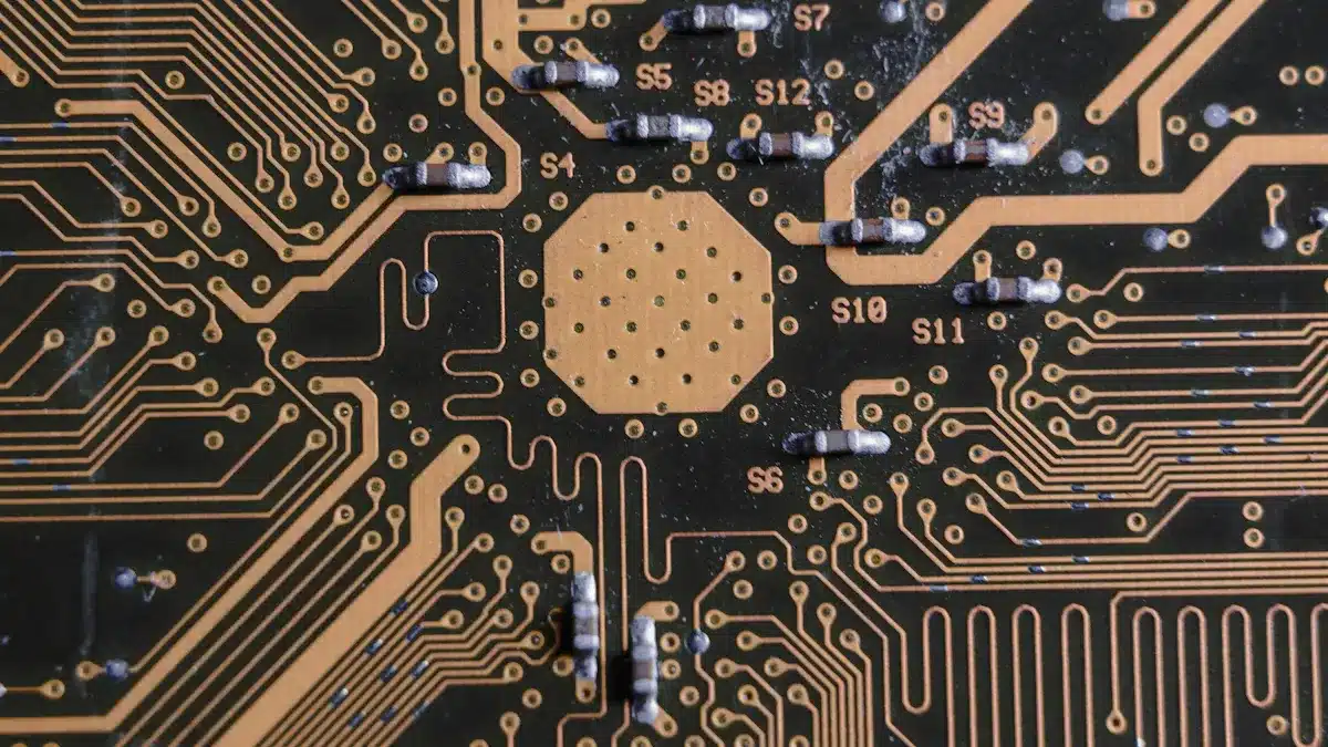
Rigid PCBs
Rigid PCBs are the most common type you will see. They have a solid base that gives support to electronic parts. These boards are often used in consumer electronics because they are reliable and affordable. Common uses include:
Communication devices like smartphones, tablets, and radios.
Computers for personal and business tasks.
Entertainment systems such as TVs and video game consoles.
Home appliances like refrigerators and microwaves.
These uses show the need for small, dependable PCBs that can manage complex electronic tasks in everyday items.
Flexible PCBs
Flexible PCBs have special benefits that rigid boards do not. They can bend, twist, and fit into different shapes without breaking connections. This flexibility allows for creative designs, especially in wearable and medical devices. Here’s how flexible PCBs help these areas:
Feature/Advantage | Description | Impact on Wearable and Medical Devices |
|---|---|---|
Flexibility and Bendability | Flexible PCBs can bend and twist without breaking. | They fit comfortably on the body and in tight spaces. |
Miniaturization (Space & Weight) | They are thinner and lighter than rigid PCBs. | This is important for small, lightweight wearable devices. |
Durability and Reliability | They can handle bending and shock well. | This makes them good for devices that move a lot. |
Improved Signal Integrity | Consistent properties improve signal quality. | This ensures clear data transfer in medical monitoring devices. |
Rigid-Flex PCBs
Rigid-flex PCBs mix the best parts of rigid and flexible boards. They have stable areas for mounting and flexible parts that work like hinges. This design allows for complex 3D shapes and makes assembly easier by removing connectors. Rigid-flex PCBs are great for places where space is tight and reliability is very important.
Knowing these PCB types helps you pick the right one for your project. Each type has unique features that can greatly affect how well your electronic devices work.
PCB Manufacturing Process
The PCB manufacturing process has several important steps. These steps change your electronic design into a working printed circuit board. Knowing these steps is key for good quality and efficiency in making PCBs. Here’s a clear overview of the process:
Design and Layout
The first step in the manufacturing of a PCB is making a schematic diagram with special software. You pick components and follow design rules to make sure it works. Next, you create the PCB layout design. Here, you arrange components and connect pathways. Think about layer count, trace width, and where to place components. After this, you generate Gerber files. These files have all the information needed for manufacturing. Doing design rule checks (DRC) helps find mistakes early.
Material Selection
Picking the right materials is very important for how long your PCB lasts and how well it works. Here are some things to think about:
Material Properties: Check for features like dielectric constant and thermal expansion coefficient.
Thermal Management: Look at things like glass transition temperature (Tg) to make sure the material can handle heat.
Manufacturing Compatibility: Choose materials that fit with your manufacturing process. For example, FR-4 is common for surface mount technology.
Environmental Conditions: Think about humidity and temperature changes.
Frequency Requirements: For high-frequency uses, pick materials with low dielectric loss.
These points help make sure your materials are strong and work well in the final product.
Inner Layer Imaging
After you have your design and materials, the next step is inner layer imaging. This step puts the PCB layout onto the copper-clad laminate. You use a photoengraving method, applying a photosensitive film to the copper surface. After shining UV light on it, the film hardens where you want to keep copper. The areas that are not exposed are removed, leaving the copper pattern you want.
Etching Process
The etching process takes away unwanted copper from the PCB. You dip the board in a chemical solution that dissolves the exposed copper. The type of etching chemicals you use can greatly affect how eco-friendly PCB manufacturing is. Traditional chemicals often have harmful substances, while biodegradable solutions are better for the environment. This step is key for shaping the conductive pathways on your PCB.
Photoresist Stripping
After etching, you must remove the leftover photoresist material. This step makes sure only the copper you want stays on the board. You usually use a solvent or chemical solution to strip away the photoresist, showing the etched copper traces below.
Drilling and Plating
The last steps in the PCB manufacturing process are drilling holes for components and vias. You need to align the drill holes correctly to avoid connection problems. After drilling, you use a plating process to cover the holes with copper. This step makes sure all layers of the PCB are connected electrically.
Quality Assurance in PCB Manufacturing
Quality assurance is very important in the PCB manufacturing process. It makes sure your circuit boards meet the right standards and work properly. Using good quality checks helps you avoid problems, save money, and make better products. Here are some key parts of quality assurance in PCB manufacturing.
Inspection Techniques
You can use different inspection techniques to find faults in printed circuit boards before they are fully assembled. Here are some common methods:
Visual Inspection: This cheap method relies on people to spot clear defects, like missing parts or dirty solder. It is quick but might miss hidden problems, especially in small devices.
Automated Optical Inspection (AOI): AOI uses lights and cameras to take pictures of solder joints and parts. It quickly finds defects like solder bridges and misalignment. However, it cannot check hidden solder joints, like BGA or J-lead connections.
Automatic Laser Test (ALT) Measurement: This method uses lasers to measure the height and shape of solder joints. It is great for checking solder paste amount and alignment before putting on components.
X-ray Fluoroscopic System: This system uses X-rays to create images of solder joint thickness and inside quality. It finds problems like cracks and not enough solder, especially on single-sided PCBs.
X-ray Lamination System: This advanced method makes detailed images of solder joints by scanning through layers. It allows for close inspection of both front and back side solder joints, including BGA and PTH joints.
These inspection techniques help you find defects early in the manufacturing process, ensuring better quality and reliability in your PCBs.
Testing Methods
After inspection, you need to use different testing methods to check if your PCBs work correctly. Here are some common testing approaches:
Functional Testing: This method checks if the PCB does what it is supposed to do. You apply power and test the circuit under normal conditions.
In-Circuit Testing (ICT): ICT tests individual parts on the PCB while it is still connected. This method helps find faulty parts and checks proper connections.
Boundary Scan Testing: This technique uses built-in test circuits to check connections between parts. It is especially useful for finding faults in complex PCBs.
Environmental Testing: You can expose PCBs to different conditions, like temperature and humidity, to see if they can handle real-world use.
Using these testing methods helps you confirm the performance and reliability of your PCBs, lowering the chance of failures later.
Compliance Standards
Following compliance standards is key for making sure your PCBs are safe and high quality. Different organizations set these standards to help manufacturers. Some important standards include:
IPC Standards: The Institute of Printed Circuits (IPC) gives guidelines for PCB design, manufacturing, and assembly. Following IPC standards helps ensure consistency and quality.
ISO 9001: This international standard focuses on quality management systems. Getting ISO 9001 certification shows your commitment to quality and customer satisfaction.
RoHS Compliance: The Restriction of Hazardous Substances (RoHS) rule limits the use of certain harmful materials in electronic products. Ensuring RoHS compliance helps protect the environment and public health.
By following these compliance standards, you can improve the quality of your PCBs and build a strong reputation in the industry.
Final Steps in PCB Production
Solder Mask Application
After you finish drilling and plating, you put on a solder mask. This mask protects the copper traces. It stops solder from connecting the pathways during assembly. You can pick different colors for the solder mask, but green is the most popular. To apply it, you coat the PCB with a liquid photoimageable solder mask. Then, you shine UV light on it. This light hardens the mask where you want it. Finally, you wash away the parts that were not exposed. This leaves a protective layer over the copper.
Surface Finish
Next, you add a surface finish to help with soldering and protect the copper. There are several choices, including:
HASL (Hot Air Solder Leveling): This method uses hot solder to cover the copper. It gives a good surface for soldering but may not work well for tiny components.
ENIG (Electroless Nickel Immersion Gold): This finish resists corrosion well and is great for high-frequency uses. It gives a flat surface, making soldering easier.
OSP (Organic Solderability Preservative): This eco-friendly choice protects copper without adding metal. It works well for small production runs.
Choosing the right surface finish is very important for your PCB’s reliability.
Final Testing
The last step in making PCBs is final testing. You do different tests to check if the board works correctly. Functional testing sees if the PCB runs as it should under normal conditions. In-circuit testing (ICT) checks the individual parts and connections. Environmental testing puts the PCB through different conditions, like heat and humidity, to test its strength. These tests help find any problems before the PCB goes to the customer, ensuring high quality and reliability.
By knowing these final steps, you can see how important each stage is in making PCBs. Each step helps improve the overall quality and performance of the final product.
In conclusion, every step in making PCBs is very important. From designing to testing at the end, each part helps your PCB meet quality rules. You need to use best practices to make things work better and be more reliable. This means choosing materials carefully and testing thoroughly. Well-made PCBs can greatly boost how well electronic devices work. They help your devices run properly and last longer. By knowing these steps, you can make smart choices that lead to better products.
FAQ
What is a PCB?
A PCB, or printed circuit board, is a flat board that connects electronic parts. It creates paths for signals and power, helping devices work correctly.
How long does it take to manufacture a PCB?
The time to make a PCB depends on how complex it is and how many you need. Simple designs might take a few days, while more complicated boards can take weeks.
What materials are commonly used in PCBs?
Common materials for PCBs are FR-4, which is a fiberglass epoxy, and polyimide for flexible boards. These materials are strong and have good electrical properties.
Can I design my own PCB?
Yes, you can create your own PCB using special software. Many tools are available for both beginners and experts, letting you make custom layouts.
What are the main applications of PCBs?
PCBs are used in many areas, like consumer electronics, car systems, medical devices, and industrial machines. They are important for today’s technology.
See Also
An In-Depth Overview Of PCBA Manufacturing Procedures
Detailed Walkthrough Of The PCBA Production Process
Key Stages In The PCBA Assembly And Fabrication