
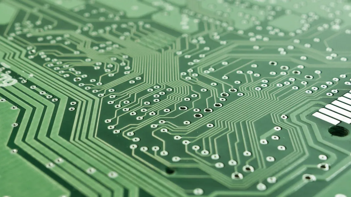
PCB fab and assembly are two crucial steps in the production of electronics. PCB fab refers to the process of creating bare printed circuit boards, which are the physical foundation for electrical connections but do not yet contain any electronic components. PCB assembly, on the other hand, involves soldering and attaching electronic parts onto these fabricated boards, resulting in fully functional electronic modules.
Understanding the distinction between pcb fab and assembly is essential for effective project planning. The global PCB assembly market was valued at USD 73.1 billion in 2023 and is projected to reach USD 96.2 billion by 2031, highlighting the significant role pcb fab and assembly play in the electronics industry.
Key Takeaways
PCB fabrication makes the basic circuit board. It does this by layering materials, drilling holes, and etching copper paths.
PCB assembly puts electronic parts on the board. This is done through soldering, which makes the board work.
Picking the right materials and parts affects quality, cost, and performance of PCBs.
Fabrication usually costs less and takes less time. Assembly costs more and can take longer because of parts sourcing.
Fixing problems like soldering defects and thermal issues early helps make the final product more reliable.
PCB Fabrication
Fabrication Process
The PCB fabrication process has important steps. These steps change design files into working printed circuit boards. This process is key to making sure the final product is good quality and meets standards. Top manufacturers usually do these steps:
Design and File Preparation: Designers use special software to make the circuit layout. They then save the design files, often in Gerber format, which acts as the guide for making the boards.
Drilling: Drills controlled by computers make holes for vias and where parts will go, based on the design files.
Plating and Copper Deposition: A thin layer of copper goes over the panel and inside the drilled holes. This creates electrical connections between layers.
Outer Layer Imaging: Photoresist is put on, and UV light hardens it through film masks. This shows where the copper pathways will be on the outer layers.
Final Etching: Unwanted copper is removed with chemicals, leaving only the designed copper traces.
Solder Mask Application: An epoxy solder mask is put on and cured with UV light. This protects the board and stops solder bridges.
Surface Finish: Extra plating, like gold or silver, is added to improve soldering.
Electrical Testing: The finished PCB is tested carefully to check circuit integrity and functionality.
This organized method makes sure the PCB fabrication process creates high-quality printed circuit boards for many uses.
Materials for PCB Fabrication
The materials chosen greatly affect how well and how much fabricated PCBs cost. Here are some common materials used in PCB fabrication:
Material | Description | Key Properties |
|---|---|---|
FR4 | Most common PCB material; woven fiberglass and epoxy resin composite | Flame retardant, high mechanical strength, excellent electrical insulation, thermal resistance |
CEM-1 | Paper-based core with a single copper layer | Economical, used for simple single-layer PCBs |
CEM-3 | Epoxy layer with paper base | Better mechanical properties than CEM-1, used for multi-layer PCBs |
Polyimide (PI) | High-performance flexible material for flexible PCBs | Highly flexible, excellent thermal stability, chemical and mechanical resilience |
PTFE (Teflon) | Used for high-frequency PCBs, especially RF applications | Low dielectric constant, excellent chemical resistance, ideal for high-frequency applications |
Metal Core PCB | Uses metal base (usually aluminum) for heat dissipation | Superior heat dissipation, robust mechanical strength, ideal for power-intensive applications |
FR4 is still the most popular choice because it is cost-effective and strong. However, advanced materials like polyimide and PTFE are becoming more popular for high-frequency uses. These materials improve performance but can make manufacturing harder and more expensive.
Knowing the PCB fabrication process and the materials used is very important for manufacturers who want to make reliable and efficient printed circuit boards. As technology grows, the industry keeps looking for new materials that boost performance while also caring for the environment.
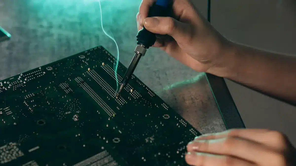
PCB Assembly
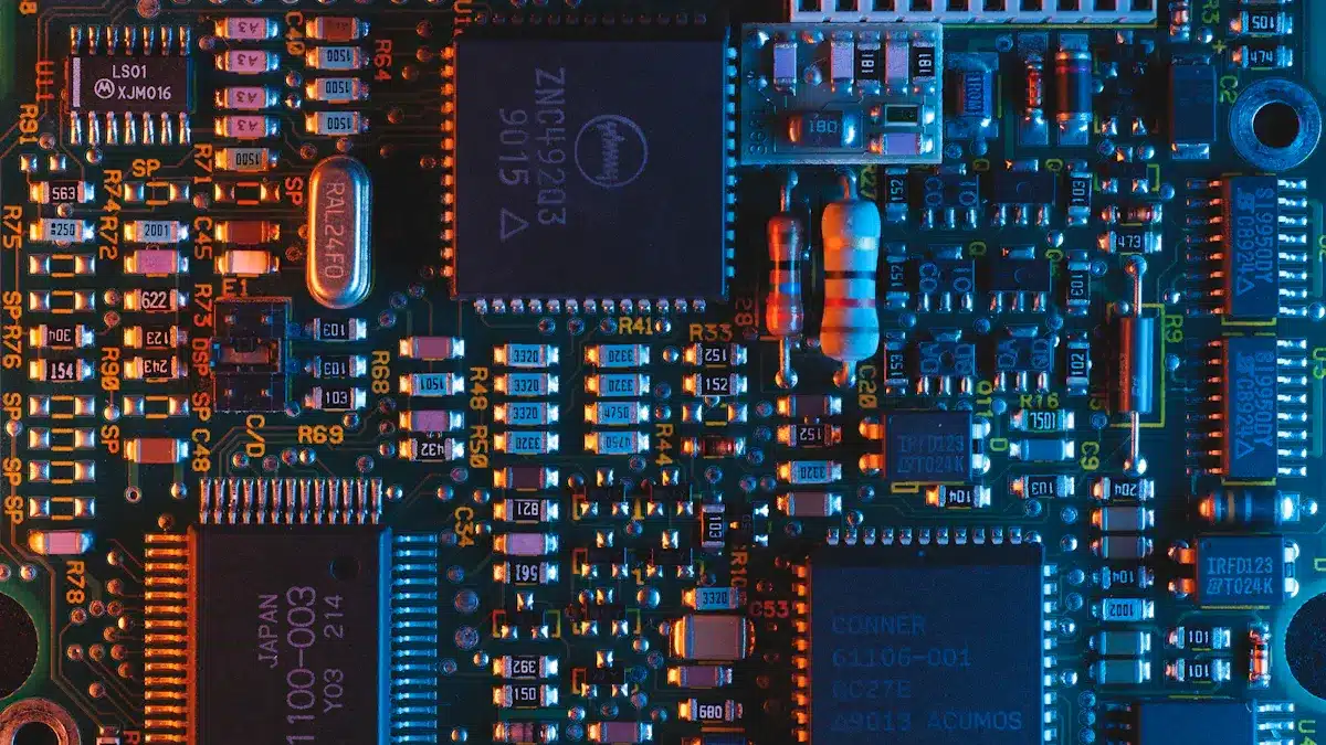
The PCB assembly process changes bare printed circuit boards into working electronic devices. This process is very important. It affects how reliable and well the final product works. A good assembly makes sure all parts work together smoothly. This is key for how well the device functions.
Assembly Process
The assembly process has several main steps that manufacturers follow to keep quality and efficiency high. These steps are:
Design for Assembly (DFA): Manufacturers check design files, like Gerber and Bill of Materials (BOM), to make sure parts are placed correctly.
Surface Mount Technology (SMT) Assembly:
Solder paste is applied using stencils.
Inspect solder paste deposits to check for accuracy.
Place surface mount parts using machines that pick and place.
Reflow soldering is done to hold parts in place.
Through-Hole Part Insertion: This step includes putting through-hole parts in by hand, then soldering them, often using wave soldering.
Final Inspection and Cleaning: This checks that the board has no defects and cleans off extra solder or dirt.
Assembly drawings and notes help guide the PCB assembly process. These documents show where parts go, reference designators, and soldering needs. They help prevent mistakes during assembly and make sure everything meets IPC standards, which set rules for mounting and acceptance.
Components for PCB Assembly
The parts used in printed circuit board assembly are very important for how well the final product works. Here are some common types of components:
Component Category | Examples and Functions |
|---|---|
Passive Components | Resistors (control current), Capacitors (hold charge), Inductors (store energy in a magnetic field). |
Active Components | Diodes (allow current to flow one way), Transistors (boost signals, act as switches). |
Integrated Circuits | Complex chips that handle data processing and memory storage; act as the brain of the device. |
Sensors | Change physical inputs (light, heat, motion) into electrical signals; types include proximity and temperature sensors. |
Connectors | Join wires or cables; can be surface mount or through-hole for strength. |
Choosing the right parts is very important. Parts must meet electrical needs, like voltage and current ratings, for reliable operation. Mechanical and environmental needs, like temperature range and humidity resistance, are also key for long-lasting reliability.
The choice between surface mount technology (SMT) and through-hole technology (THT) impacts the assembly process. SMT allows for smaller parts and more density, while THT gives stronger mechanical bonds, making it better for tough applications.
Key Differences Between PCB and PCBA
Process Comparison
The steps in PCB fabrication and assembly are very different. PCB fabrication makes the physical board. PCB assembly adds electronic parts to that board. Here are the main differences:
PCB Fabrication:
It layers materials, etches copper paths, drills holes, and puts on solder masks.
It needs skills in materials science, chemical processes, and precise machining.
Quality checks include electrical tests, automated optical inspection (AOI), and X-ray scans.
It creates the bare board, which is the base for electronic circuits.
PCB Assembly:
It gets electronic parts, places them correctly on the board, and solders them.
It requires knowledge of circuit design, soldering methods, and how parts work.
Quality checks include functional testing, in-circuit tests, and visual inspections.
It makes the PCB work by adding components.
The link between PCB and PCBA is very important. Fabrication sets the stage, while assembly makes the design real.
Cost and Time Factors
Cost and time also differ between PCB fabrication and assembly. Knowing these differences helps with project planning.
PCB Fabrication Costs:
Usually lower and more predictable.
Costs depend on materials, number of layers, and how many are made.
For example, using FR-4 material is cheap, but special materials like Rogers cost more.
Average costs can be from $1 to $10 per square inch, based on complexity.
PCB Assembly Costs:
Often higher and more variable.
Costs depend on sourcing parts, labor, assembly methods (surface mount vs. through-hole), and testing.
Assembly costs can range from $5 to $50 per board, based on complexity and volume.
Assembly usually makes up 30% to 60% of total production costs.
For lead times, PCB fabrication usually takes 3 to 7 days. Assembly can take longer due to part availability and supply chain issues. For example, assembly may take longer if parts are not easy to find.
Cost Aspect | PCB Fabrication | PCB Assembly |
|---|---|---|
Average Cost Range | Generally lower and more predictable | |
Cost Drivers | Material costs, layer count, process complexity | Labor, component sourcing, assembly methods |
Cost Proportion | Lower portion of total product cost | Accounts for 30% to 60% of total production cost |
Volume Effect | Higher quantities reduce unit fabrication cost | Economies of scale reduce assembly cost per unit |
Knowing these key differences between PCB and PCBA helps manufacturers make smart choices about their projects. By understanding each process’s unique parts, they can better plan for costs and timelines.
PCB Fab and Assembly Challenges
Challenges in Fabrication
PCB fabrication has many challenges that can affect how good and reliable the final product is. Some common problems are:
Mechanical Challenges: Boards can warp, layers can misalign, and tiny cracks can form. This happens because different materials expand at different rates when heated. Thin or large PCBs are more likely to bend, which can cause parts to misalign or break.
Thermal Management Issues: Getting rid of heat can be hard, especially in crowded designs. Heat stress from heating and cooling can damage parts and weaken solder joints.
Signal Integrity Problems: If components are not placed correctly, it can cause electromagnetic interference (EMI). This leads to noise and timing problems.
Component Placement Difficulties: When parts overlap or there isn’t enough space, it makes routing harder and increases the chance of solder bridges.
To fix these challenges, manufacturers can:
Choose materials that expand at similar rates to reduce stress.
Add design features like rounded corners and curved traces to spread out stress evenly.
Use conformal coatings to protect against moisture and temperature changes.
Improve component placement by grouping similar parts and keeping enough space.
Challenges in Assembly
PCB assembly has its own challenges too. Some common issues are:
Solder Bridging: This happens when solder makes unwanted connections between parts.
Insufficient Solder: Weak or shaky connections can occur if there isn’t enough solder.
Component Misalignment: If parts are not placed right, it can cause the device to fail.
Thermal Issues: Overheating can harm parts, especially in tightly packed boards.
To solve these assembly challenges, manufacturers should:
Use precise manufacturing methods to find and fix defects.
Apply strict quality control measures, like visual checks and automated tests.
Simplify PCB designs and reduce the number of components.
Make sure parts are placed accurately to avoid misalignment and soldering problems.
By tackling these challenges early in design and manufacturing, companies can make their PCBs and PCBA more reliable and effective.
In conclusion, PCB fabrication and assembly have different but connected jobs in making electronics. PCB fabrication is about making the bare circuit board by layering materials and etching copper. On the other hand, PCB assembly is about putting and soldering electronic parts onto the board to make it work.
Knowing these differences is important for doing projects well. When deciding between fabrication and assembly, think about cost, quality, and how long it takes. Look at what your project needs to get the best results.
Key Considerations:
Quality control measures
Lead time and delivery reliability
Customer support responsiveness
By remembering these points, manufacturers can make smart choices that improve their production processes.
FAQ
What is the main difference between PCB fabrication and assembly?
PCB fabrication makes the bare circuit board. PCB assembly adds electronic parts to that board. Fabrication focuses on materials and steps. Assembly is about placing parts and soldering them.
How long does the PCB fabrication process typically take?
The PCB fabrication process usually takes 3 to 7 days. Things like complexity, material choice, and how many are made can change the time.
What materials are commonly used in PCB fabrication?
Common materials are FR4, CEM-1, CEM-3, polyimide, PTFE, and metal core substrates. Each material is used for different needs based on performance, cost, and heat properties.
Why is quality control important in PCB assembly?
Quality control makes sure all parts work right and meet design needs. It helps stop defects, cuts down failures, and improves the final product’s reliability.
How do costs differ between PCB fabrication and assembly?
PCB fabrication costs are usually lower and more predictable. Assembly costs can change a lot based on labor, parts, and methods. Assembly often makes up 30% to 60% of total production costs.
See Also
A Comprehensive Guide To PCBA Manufacturing And Assembly
Examining Functional And Structural Variations Between PCB And PCBA
Key Distinctions Between PCB And PCBA In Electronics Production
Understanding SMT Process Steps In PCBA Assembly Manufacturing
Unveiling Lesser-Known Differences Between PCBA And PCB Boards