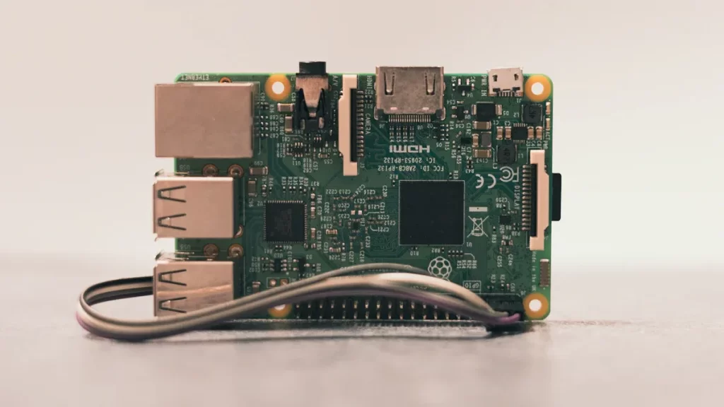

Industrial IoT gateway PCB assembly is key to modern systems. It helps connect devices, process data, and share information easily. Without it, IoT gateways wouldn’t work well in tough settings. Good assembly ensures strong performance and reliability for heavy tasks. It also lets you grow your IoT network as your needs increase.
Strong PCB assembly helps you get the most from your Industrial IoT systems.
Key Takeaways
Strong PCB assembly is important for Industrial IoT gateways. It helps devices connect well and share data easily.
Testing is very important. It finds problems early so the PCB works well and lasts longer.
Good design and part placement make devices work better. Focus on strong signals and cooling to keep them reliable in hard conditions.
Scalability helps IoT networks grow. Good PCB assembly makes adding parts easy without lowering performance.
Saving money is possible by using common parts and machines. This keeps production cheap while keeping good quality.
The Role of Industrial IoT Gateway PCB Assembly
Helping Devices Stay Connected
Industrial IoT gateway PCB assembly helps connect devices in your network. It makes sure sensors, actuators, and parts work together smoothly. The assembly includes important hardware like microcontrollers and communication tools. These let devices share data without stopping or slowing down.
You get better connections because the PCB assembly improves signals and reduces delays. For example, machines in a factory can share live data easily. The PCB assembly keeps the information flowing without problems. This is very important for keeping factories running well.
Making Data Work and Communicate
PCB assembly helps process data by adding processors and memory. These parts handle the large amounts of data your devices create. The assembly makes sure the gateway works fast and correctly, so you can make smart choices.
It also helps with communication. The PCB assembly includes tools like Wi-Fi, Ethernet, and Bluetooth. These let your gateway send data to the cloud or other devices. With good communication, you can control and check your systems from anywhere. This makes your work more efficient.
Growing with Your IoT Network
When your IoT network gets bigger, you need it to grow easily. PCB assembly helps by allowing more parts and features to be added. You can make your network larger without losing performance.
Scalability shows how good PCB assembly helps. For example:
What It Means | |
|---|---|
Response Times | How fast the system answers requests, showing how efficient it is. |
Throughput Rates | How much data is handled in a set time, showing its capacity. |
Resource Use | How well the system uses its resources, showing its effectiveness. |
These metrics prove that PCB assembly helps your gateway handle more work. By staying efficient, it supports your growing IoT network.
Key Steps in the Industrial IoT Gateway PCB Assembly Process
PCB Design and Layout for IoT Applications
Designing a PCB for IoT needs careful planning. Each step ensures it works well for Industrial IoT systems. Here’s how to do it:
Know What Your Application Needs: Figure out what your IoT system requires. Think about size, communication, and environment.
Pick and Arrange Parts: Use small, energy-saving parts. Place them to avoid interference and boost performance.
Improve Wireless Signals: Focus on where wireless parts go. Good antenna spots and strong signals are key.
Keep Signals Strong: Use methods like matching impedance and shorter paths for better signals.
Save Power: Choose low-power parts and design for energy saving. This is vital for devices that run all the time.
Make It Easy to Build: Follow rules to make the PCB simple and cheap to produce.
Prepare for Tough Conditions: Design the PCB to handle heat, cold, or moisture.
Test Everything: Check for mistakes and fix them before finishing.
Follow Rules: Make sure the PCB meets safety and legal standards.
By doing these steps, you can build a PCB that works well and lasts long in Industrial IoT systems.
Smart Placement of Components
Placing parts on a PCB needs care and skill. Good placement helps the IoT gateway work well, even in tough places.
For example, if your gateway connects many sensors in a factory, you might face problems like signal interference or heat. To solve these, you can:
Problem | Fix |
|---|---|
Signal Interference | Place parts to reduce interference. Add shields if needed. |
Heat Issues | Use tools to plan where hot parts go. Add heat sinks or special holes. |
Tough Conditions | Use strong materials and protective coatings to keep the PCB safe. |
These fixes help your PCB handle hard jobs while staying reliable.
Soldering and Assembly for Strong Connections
Soldering and assembly are important for keeping parts attached to the PCB. Good soldering makes sure parts stay in place, even under stress.
To do this, manufacturers use advanced checks, like:
Automated Optical Inspection (AOI): Cameras check for bad solder joints. This ensures the PCB meets quality standards.
X-Ray Inspection: X-rays check hidden solder joints under parts like BGAs. They make sure there are no big gaps.
Temperature Tests: These tests heat and cool the PCB to find weak spots in solder joints.
Other tests, like shaking and vibration tests, check if the PCB can handle rough conditions. By focusing on good soldering and assembly, you can make a PCB that works well for a long time.
Quality Testing to Ensure Performance Standards
Quality testing checks if your Industrial IoT gateway PCB assembly works well. It finds problems early, making sure it stays strong and reliable. By using strict tests, you can trust your PCB assembly to work in real-life situations.
Common Testing Procedures
Standard tests help find flaws and ensure the PCB lasts long:
Visual and X-ray Inspection: These tests spot surface and hidden issues, like misplaced parts or solder mistakes.
Peel Test: This test checks how strong the layers are, so the PCB can handle stress.
Automated Optical Inspection (AOI): AOI uses cameras to find problems, like missing parts or bad soldering.
Key Testing Categories
Each test looks at a specific part of how the PCB works. The table below shows important tests and their goals:
Testing Procedure | Description |
|---|---|
Makes sure the PCB works as it should with electricity. | |
Environmental Stress Testing | Tests the PCB in tough conditions to check its strength. |
Cleanliness Testing | Checks that the PCB is clean and free of harmful dirt. |
What to Look for During Testing
When testing, focus on these important things to keep quality high:
Rules for checking and testing
Results and reports from the tests
Notes on problems and how they were fixed
Records showing testing tools are working correctly
By watching these details, you can fix problems before they hurt your PCB’s performance.
Tip: Keep your testing tools and methods updated to meet new standards.
Good quality testing not only follows rules but also makes your IoT gateways last longer. This step is key for keeping devices connected and data flowing in tough industrial settings.
Benefits of High-Quality Industrial IoT Gateway PCB Assembly
Better Performance in Tough Workplaces
Good PCB assembly makes IoT gateways work better. It uses smart technology to improve signals and save space. For example, small parts are built into the PCB to make it more efficient. High-Density Interconnect (HDI) technology adds more circuits, helping devices handle hard tasks. These upgrades make sure your gateways work well in busy industries.
The table below shows key technologies and their benefits:
Technology/Method | Description | Benefits |
|---|---|---|
Embedded Components | Adds small parts directly into the PCB. | Makes signals better and saves space. |
High-Density Interconnect (HDI) | Uses tiny lines and layers for more circuits. | Fits more circuits for powerful devices. |
Improved Thermal Management | Uses special materials to manage heat. | Keeps devices safe in high-power jobs. |
Smart Factory and Industry 4.0 | Adds IoT and AI to factories. | Boosts efficiency and prevents downtime. |
Using these technologies makes your gateways stronger and more reliable in tough places.
Stronger and Longer-Lasting Gateways
Gateways need to last in harsh conditions. High-quality PCB assembly helps by placing parts carefully and managing heat well. This lowers the chance of problems and makes gateways last longer.
The table below shows how advanced assembly improves reliability:
Benefit | Description |
|---|---|
Machines place parts with high accuracy. | |
Yield Improvement | Automated systems reduce mistakes and rework. |
Thermal Control | Heat is managed carefully during soldering. |
Zero Defects | Error rates are very low, ensuring reliable boards. |
With fewer mistakes and better heat control, your gateways stay dependable for a long time.
Easy Growth for Expanding IoT Needs
As IoT grows, scaling up is important. Good PCB assembly helps manufacturers adjust quickly. Automation allows faster production and more product options. This means your gateways can grow without losing quality.
Here are some facts:
It may reach $616.75 billion by 2032, growing 10.77% yearly.
A strong PCB assembly process ensures fast production and good quality. This helps meet the rising demand for IoT devices while keeping performance steady.
Challenges in Industrial IoT Gateway PCB Assembly
Handling High-Density Component Placement
High-density PCBs need careful planning to work well. You must place parts, wires, and layers correctly for complex circuits. Microprocessors and memory chips need the best spots to work fast.
Here are key factors for successful placement:
Factor | What It Does |
|---|---|
Solder Paste Accuracy | Makes sure solder joints form correctly. |
Solder Paste Amount | Affects how strong and reliable joints are. |
Stencil Size and Thickness | Controls how much solder paste is used. |
PCB Flatness | Helps parts sit properly and keeps joints strong. |
Reflow Heat Settings | Melts and hardens solder for good connections. |
Equipment Use | Poor use causes more mistakes and waste. |
Solder Paste Brand | Impacts joint quality based on its mix. |
Board Design and Part Density | Adds challenges and risks during assembly. |
Heat-making parts need special care. Place them smartly to manage heat better. Put decoupling capacitors near power pins to cut noise. These steps keep your PCB working smoothly and reliably.
Making PCBs Tough for Harsh Conditions
Industrial IoT gateways often face tough environments. Strong materials and designs help them survive. For example, polyimide PCBs handle heat and stress well. These are great for aerospace, cars, and factories.
Panasonic tested materials in space-like conditions. They stayed strong with no changes in looks or performance.
Through-hole parts make PCBs stronger. They attach firmly to the board, handling stress better than surface-mount parts. These parts also work well with high-heat soldering, making them perfect for industrial use.
Fixing Signal Problems and Interference
Signal problems and interference are big issues in PCB assembly. Bad signals can lose data, and interference can mess up communication. Testing and smart designs can solve these problems.
Test Type | What It Checks | Example Problem | Where It’s Used |
|---|---|---|---|
RF Interference Test | Checks if power and data lines resist RF noise | A device resets when RF noise hits its power line | Factories, Cars |
Static Discharge Test | Simulates static electricity shocks | A device freezes after a static shock | Gadgets, Medical Tools |
Power Surge Test | Tests if devices handle sudden power spikes | A device shuts down during a power surge | Power Systems, Cars |
Magnetic Field Test | Checks if devices work near magnetic fields | Errors happen in devices near big motors | Factories, Medical Tools |
Voltage Dip Test | Tests if devices handle brief power drops | A sensor restarts during a short power dip | IoT, Smart Buildings |
By designing better PCBs and using advanced tests, you can avoid these problems. This helps IoT gateways stay reliable and communicate well in tough places.
Balancing Cost and Time Efficiency
Balancing cost and time is important for making IoT gateways. Smart strategies help save money while keeping good quality.
Using common parts is a smart way to cut costs. These parts are easy to find, affordable, and work well. Buying in bulk lowers the price even more. For example, ordering many parts at once makes each part cheaper, saving money over time.
Testing small batches of designs helps find problems early. This avoids expensive mistakes during big production runs. Planning for future growth also saves time and money by preventing delays later.
Automation speeds up repetitive tasks and reduces errors. Machines work fast and accurately for large jobs. For smaller or tricky tasks, manual assembly is still a good choice. Mixing both methods balances cost, speed, and accuracy.
Testing is also key to saving time and money. Designing PCBs to be easy to test makes the process faster and cheaper. Automated checks, like 3D solder paste tests, catch problems early. This reduces waste and fixes issues before they grow.
The table below shows ways to improve cost and time efficiency:
Strategy | Benefit |
|---|---|
Use Common Parts | Affordable and easy to find. |
Discounts lower overall costs. | |
Test Small Batches | Finds problems early, saving money later. |
Use Automation | Speeds up big jobs and reduces mistakes. |
Manual Assembly for Small Jobs | Cost-effective for tricky or small tasks. |
Design for Easy Testing | Makes testing faster and cheaper. |
Improve Test Procedures | Cuts extra steps to save time and money. |
By following these tips, you can make IoT gateways that are affordable and ready to use.
Industrial IoT gateway PCB assembly helps devices connect and share data. It ensures gateways work well, last longer, and grow with needs.
The global market shows why it matters:
New tech like 5G and AI needs smaller, faster PCBs.
More smart home gadgets increase demand for better PCB designs.
Electric cars need PCBs for battery and control systems.
By solving assembly problems, you can create gateways that work in tough places and support growing IoT networks.
FAQ
What is PCB assembly in Industrial IoT gateways?
PCB assembly means putting and soldering parts onto a circuit board. It helps IoT gateways connect devices, handle data, and share information well. Good assembly makes them work better and last longer in tough places.
Why is quality testing important in PCB assembly?
Quality testing checks if the PCB works properly. It finds problems early to stop failures later. By testing for electricity, strength, and cleanliness, you can trust your IoT gateway to work well.
How does PCB assembly support scalability in IoT networks?
PCB assembly lets you add more parts and features easily. It uses smart designs like HDI to handle more data and devices. This helps your IoT network grow without slowing down.
What challenges arise in Industrial IoT PCB assembly?
Challenges include placing many parts close together and making them strong for tough places. Fixing signal problems and keeping costs low also need careful planning and smart ideas.
How can you reduce costs in PCB assembly?
You can save money by using common parts and buying in bulk. Automating tasks and testing small batches first also help avoid costly mistakes.
Tip: Design for future growth early to save money later.
See Also
The Role of PCBA in Advancing Today’s Electronics
Why PCBA Manufacturing Skills Are Crucial for Electronics
The Significance of Tailored PCBA for Contemporary Electronics
Exploring Flex PCBA: Benefits and Obstacles in Electronics
Understanding PCBA Applications in Everyday Consumer Electronics