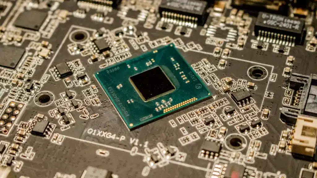

In 2025, learning PCB manufacturing assembly techniques is very important. This is true for anyone working with electronics. The need for PCB manufacturing assembly services is expected to grow significantly, potentially reaching about USD 38.5 billion by 2032. This growth is driven by new technology in consumer electronics, cars, and IoT devices. Staying up to date with the latest trends and methods in PCB manufacturing assembly is essential. Advances in technology, such as miniaturization and automation, increase the demand for improved assembly methods. Understanding these changes will help you succeed in the competitive world of PCB manufacturing assembly.
Key Takeaways
Use better soldering and inspection tools. These include AI machines and Automated Optical Inspection. They help make things more precise and reduce mistakes.
Follow a clear assembly process. First, apply solder paste carefully. Then, place components accurately with machines. Finally, control the reflow soldering temperature for strong joints.
Stop common problems like soldering mistakes and component misalignment. You can do this by regularly calibrating machines, having good designs, and using quality control methods like X-ray and In-Circuit Testing.
Design your PCB to be easy to make. Simplify layouts, work with manufacturers early, and use panelization to save time and money.
Keep learning through training and industry updates. This helps you stay ahead in PCB assembly and adapt to new technologies and trends.
Essential Tools for PCB Assembly
When you do PCB assembly, having the right tools is very important. Here’s a list of the tools you should think about.
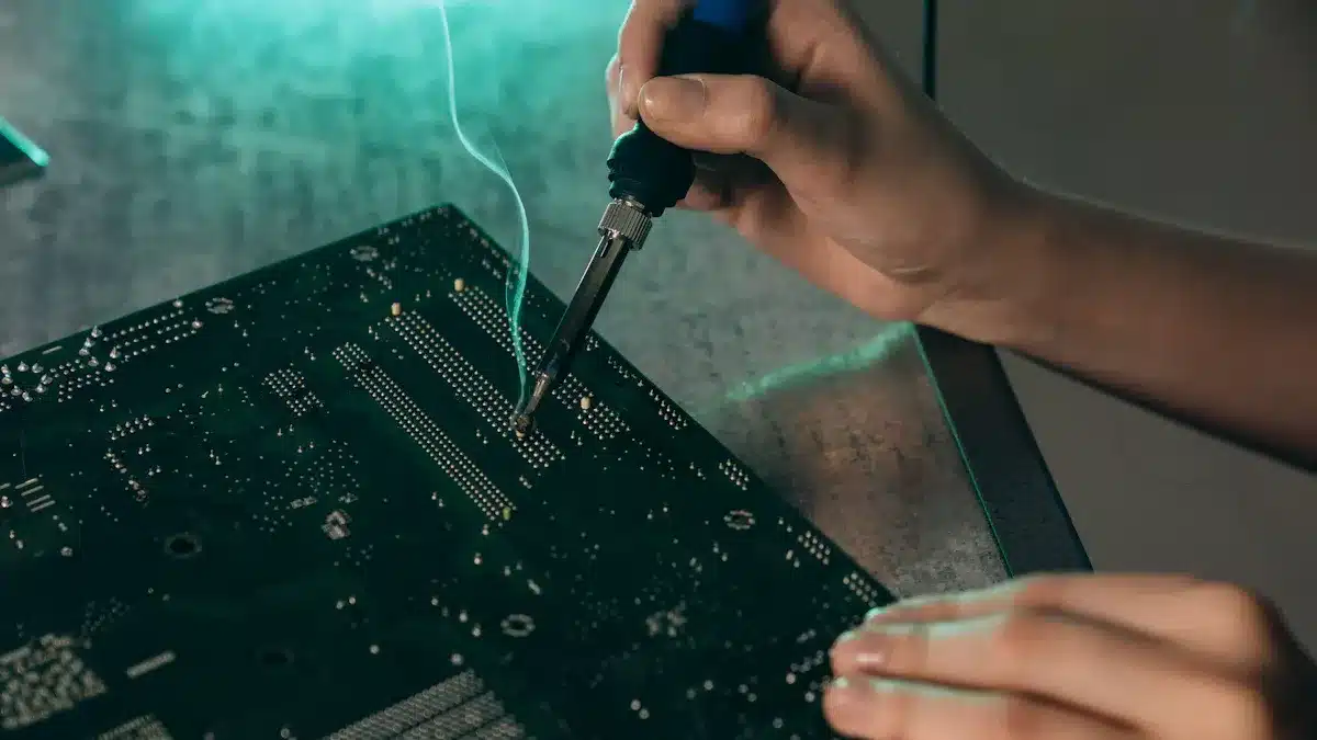
Soldering Tools
Soldering tools are key in the assembly process. Here are some important soldering tools for 2025:
Description and Role in PCB Assembly 2025 | |
|---|---|
Solder Paste Printing Machine | Puts solder paste exactly on SMD pads using stencils; AI helps reduce waste and makes sure it’s even. |
Advanced Glue Dispensing Machine | Places glue dots to stop parts from moving during reflow; adjustable settings prevent glue spills. |
High-Efficiency Reflow Soldering Machine | Uses thermal profiling and machine learning to manage temperature zones, making strong bonds and lowering defects. |
Automated Optical Inspection (AOI) System | Uses high-res cameras and AI to find problems like micro-cracks and misalignments early in assembly. |
Functional Validation Test (FVT) Systems | Runs software tests on assembled PCBs to check real-world performance with flexible options. |
These tools improve precision and efficiency, making your PCB assembly easier.
Assembly Workstations
Your assembly workstation affects how well you work. Modern workstations have features that help your workflow:
Equipment | Key Features and Impact on PCB Assembly Efficiency and Accuracy |
|---|---|
Robotic arms/vacuum nozzles place parts accurately down to 0.01 mm; can handle over 100,000 parts each hour. Calibration keeps accuracy steady. | |
Reflow Oven | Uses controlled heat profiles to create strong solder joints; multiple heating zones ensure even heating, stopping defects. |
Automated Optical Inspection (AOI) | Uses high-resolution cameras to quickly find misaligned or missing parts and solder issues; 3D imaging checks solder joint height. |
SMT Rework Station | Allows careful repair of problems using hot air and soldering irons; features like split-vision systems stop damage during repairs. |
Investing in comfortable workstations can also improve operator safety and comfort, leading to better productivity.
Inspection Equipment
Quality checks are very important in PCB assembly. The right inspection tools help you find problems early:
Automated Optical Inspection (AOI): Uses high-resolution cameras to quickly and accurately find surface problems. This method works well for high-volume production.
X-ray Inspection (AXI): Important for multilayer PCBs, this method finds hidden problems like solder voids and misalignments.
In-Circuit Testing (ICT): Automated testing checks electrical properties of parts, making sure they work before final assembly.
Choosing the right inspection method depends on how complex your PCB is and what you need for production. By adding these tools to your assembly process, you can greatly improve the quality and reliability of your PCBs.
Step-by-Step Assembly Process
The PCB assembly process has several important steps. Each step is key to making sure the final product is good and works well. Here’s a simple guide to the main steps in the assembly process:
Solder Paste Stenciling
Solder paste stenciling is the first step in assembly. You put solder paste on the PCB pads using a stainless steel stencil. This step is very important because it gets the board ready for placing components. Here are some tips to follow:
Use step stencils with different thicknesses for various component sizes. This helps get the right amount of solder paste for both small and large parts.
Clean the stencil often after every 5-10 prints to stop paste from building up and clogging.
Store stencils flat in a dry, dust-free place to keep them from warping or getting dirty.
Check stencils regularly for wear, especially around small openings, to keep paste release quality high.
Following these tips helps you avoid common mistakes, like using too much solder paste, which can cause solder bridges or shorts. Good soldering starts with a well-done stenciling process.
Pick-and-Place Techniques
After putting on solder paste, the next step is placing the components on the PCB. Automated pick-and-place machines speed up and improve this process. Here’s how they work:
These machines quickly and consistently pick parts based on PCB design coordinates.
High precision placement makes sure parts are in the right spot, reducing mistakes.
Advanced vision systems find fiducial marks and check placement accuracy.
Using automated machines can really boost your output. They can place parts at speeds up to 53,000 per hour, which is much faster than doing it by hand. This speed lets you assemble many PCBs quickly.
Reflow Soldering
The last step in the assembly process is reflow soldering. This step makes the solder joints solid and holds the components to the PCB. Here’s what you need to watch during this process:
Temperature Profiles: Adjust reflow profiles based on PCB features. Common phases include preheat, reflow, and cooling. Lead-free solder needs peak temperatures above 235 °C.
Thermal Uniformity: Make sure heat spreads evenly across the PCB to avoid local defects.
Component Orientation: Place components in a way that reduces thermal stress during reflow.
By carefully managing these factors, you can avoid problems like incomplete solder flow or component warping. Good reflow soldering is key to getting reliable joints and ensuring the overall quality of your PCB assembly.
Common Challenges in PCB Manufacturing Assembly
In PCB assembly, you might face some problems. These problems can affect how good your final product is. Knowing these challenges helps you find good solutions.
Soldering Defects
Soldering defects are common problems in PCB assembly. They can cause the final product to fail. Here are some usual soldering defects and why they happen:
Soldering Defect | Root Causes |
|---|---|
Gaps in Solder Joints | Not enough solder paste, parts not lined up right, sudden temperature changes, shaking during soldering |
Solder Balling | Dirt in solder paste (like oxides and other junk), too much heat |
Cold Solder Joints | Wrong heating (too low or too high), not enough flux |
Solder Bridging | Too much solder paste, parts not lined up right |
To fix these defects, you can use visual checks and Automated Optical Inspection (AOI) systems. These tools help you find problems early so you can fix them quickly. Regular training on good soldering methods also helps reduce defects.
Component Misalignment
Component misalignment can happen during PCB assembly. This can cause open circuits or bad joints. Here are some common reasons:
Mistakes made by people during manual assembly.
Machines not lined up right because of calibration problems.
Wrong design files that cause mismatched footprints.
To stop misalignment, use Design for Assembly (DFA) rules. Make sure footprints are correct and there is enough space. Regularly calibrate your pick-and-place machines to keep them accurate. Using AOI systems can also help check component positions after they are placed.
Quality Control
Quality control is very important in PCB assembly. It makes sure your products meet industry standards. Good quality control methods include:
Automated Optical Inspection (AOI) to find visual problems.
X-ray Inspection for hidden issues in solder joints.
In-Circuit Testing (ICT) to check if parts are placed correctly.
Using Statistical Process Control (SPC) can make your quality control even better. By watching key factors, you can spot trends and make changes before problems happen. This way, you will have fewer defects and more reliable PCB manufacturing assembly.
Combining Design with Assembly
Combining design with assembly is very important for good PCB assembly. You can make the assembly process better by focusing on three main areas: Design for Manufacturability (DFM), panelization techniques, and layout choices.
Design for Manufacturability
Design for Manufacturability (DFM) makes sure your PCB designs match what can be made. This helps avoid problems and cuts down on rework and mistakes. Here are some tips to think about:
Work with your manufacturing vendor early in the design. This teamwork helps find hidden problems before production starts.
Keep parts away from the edges of the board. This helps prevent damage, like cracks.
Don’t overcrowd the board. Making it simpler helps with testing, handling, and managing inventory.
Simplify the design by not using surface mount technology (SMT) on both sides unless you really need to. Also, avoid using tiny parts when not needed.
Pick good PCB finishes, like Electroless Nickel Immersion Gold (ENIG), instead of Hot Air Solder Leveling (HASL). This choice helps with soldering and cuts down on steps in making the board.
By using these DFM ideas, you can improve product quality and help with automation. DFM also speeds up manufacturing by letting tools work better. This leads to faster and more efficient PCB assembly.
Panelization Techniques
Panelization is a method that puts several PCBs on one panel. This technique makes the assembly process easier and has many benefits, especially for large production runs:
You can save money by reducing material waste.
Quality control stays consistent, ensuring all PCBs are the same.
It allows for large-scale production to meet industry needs.
Panelization shortens lead times, speeding up time to market.
When designing panels, think about the right panel size and material. Good spacing and layout help reduce assembly mistakes and make inspection easier. Using V-score or tab routing makes it simple to separate individual boards after assembly. By improving panelization, you can greatly enhance the cost-effectiveness of your PCB assembly, especially for bigger production runs.
Layout Considerations
The layout of your PCB affects how easy and reliable the assembly process is. Here are some layout tips to improve assembly efficiency:
Good component placement boosts assembly efficiency. Group similar parts and standardize their direction to cut down on mistakes and time.
Reduce the number of PCB layers. This makes things simpler and cheaper.
Careful routing and spacing lower signal interference and improve manufacturability.
Use thermal management techniques to keep components reliable and avoid assembly problems.
By following these layout tips, you can make production more efficient and improve product quality. A well-designed PCB layout not only makes assembly easier but also increases the reliability of your final product.
Learning PCB assembly techniques is very important for doing well in electronics in 2025. You discovered key tools, good methods, and common problems. Important points include how through-hole assembly makes products stronger and how automation helps work faster.
To keep up, think about these steps:
Work with manufacturers to create special solutions.
Read industry reports and join forums for new trends.
By always improving your skills, you can adjust to the future of PCB assembly and help with new ideas in the field.
FAQ
What is PCB assembly?
PCB assembly is when you connect electronic parts to a printed circuit board (PCB). This means soldering the parts onto the board to make working electronic devices.
Why is quality control important in PCB assembly?
Quality control makes sure your assembled PCBs meet industry standards. It helps find problems early, which lowers the chance of product failure and makes everything more reliable.
How can I improve my PCB design for assembly?
You can make your PCB design better by using Design for Manufacturability (DFM) ideas. Work with manufacturers, simplify layouts, and place components correctly to make assembly easier.
What are common soldering defects?
Common soldering defects are cold solder joints, solder bridging, and gaps in solder joints. These problems can happen because of wrong temperature control, too much solder, or parts not lining up right during assembly.
How does automation impact PCB assembly?
Automation greatly boosts efficiency and accuracy in PCB assembly. Automated machines can quickly and consistently place parts, which reduces mistakes and speeds up production times.
See Also
Effective Strategies To Improve PCB Assembly Productivity
Ten Proven Ways To Achieve Cost-Effective PCBA Assembly
A Comprehensive Guide To PCBA Manufacturing And Assembly