Imagine making advanced circuits without wasting materials or spending a lot. Multi-layer 3D printed PCBs make this happen. This new technology creates circuits one layer at a time. It only uses the exact amount of material needed. Old methods need costly tools, but 3D printing uses one printer and basic materials. You can design complex shapes and layers with great ease. This not only saves money but also makes electronics easier to build. It helps speed up production and encourages new ideas.
Key Takeaways
Multi-layer 3D printed PCBs help save time and money.
They allow fast creation of complex circuits for many uses.
This technology lets designers make unique shapes for small spaces.
It works well for different industries needing custom designs.
3D printing uses less material, which is better for the planet.
Faster prototypes with 3D PCBs help companies create new ideas quickly.
This keeps businesses ahead in a competitive market.
These PCBs are used in gadgets, medical tools, and more.
Their flexibility shows how useful 3D printed PCBs can be.
Understanding Multi-layer 3D Printed PCBs
What Are Multi-layer 3D Printed PCBs
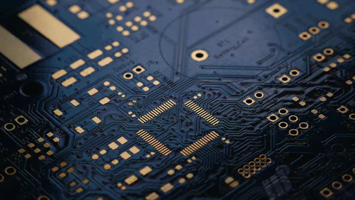
Multi-layer 3D printed PCBs are special circuit boards made with 3D printers. Unlike old methods that remove material, 3D printing adds layers step by step. These layers include paths for signals, power areas, and protective coatings. Stacking layers helps create small designs for advanced electronics.
Each layer has its own job. Signal layers link parts together. Power and ground layers keep voltage steady. Protective layers stop rust and prevent short circuits. This layered design makes small devices work better and fit more features.
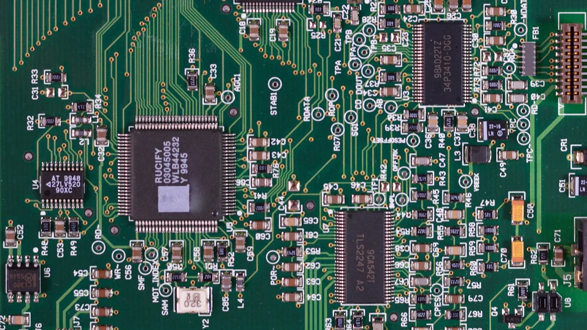
How 3D Printed Circuit Boards Differ from Traditional PCBs
3D printed PCBs are very different from regular ones. Regular PCBs need many steps like drilling and coating, which take weeks. 3D printing skips these steps and makes boards in one day. Advanced tools like Nano Dimension printers make this possible.
Another big difference is design freedom. Regular boards are flat and square. With 3D printing, you can make curved or unique shapes. Tools like Optomec’s jetting technology let you print on curved surfaces. This opens up new ways to design cool electronics.
The Process of 3D Printing Circuit Boards
Making 3D printed PCBs needs careful steps to get them right:
Plan the board layout to fit its space.
Use rules to avoid mistakes during printing.
Check design files to fix problems early.
Follow assembly rules to make building easier.
Use software to test and improve designs.
These steps help avoid common problems like bad spacing or errors. Careful planning makes boards faster to build and more reliable. Compared to old methods, 3D printing is quicker and allows more custom designs. It’s changing how electronics are made.
Advantages of Multi-layer 3D Printed PCBs
Faster Prototyping and Production
Making new electronics needs quick work. 3D printed boards help by saving time. Old methods take weeks to make one prototype. With 3D printing, you can make a model in one day. This lets you test designs fast and fix problems quickly.
Quick prototypes are very useful for research and development. They let you try new ideas and create products faster. Using 3D printing keeps you ahead in the electronics industry.
Enhanced Design Flexibility
Creating electronics needs both skill and imagination. 3D printed boards allow unique designs. Unlike flat, square boards, 3D printing makes curved or layered shapes. This gives more options for creative designs.
For example, you can make boards fit small or odd spaces. This is important for industries like aerospace and medical devices. 3D printing helps invent new ways to design electronics.
Cost-effective Manufacturing
Making electronics can cost a lot of money. 3D printed boards are cheaper to make. They use only the needed materials, saving money and reducing waste. You don’t need expensive tools or molds like old methods.
You can also make small batches without extra costs. This is great for startups or small projects. 3D printing lowers costs while keeping good quality results.
Transforming Electronics Manufacturing
Driving Innovation in Product Development
We are entering a new age of creating products. Multi-layer 3D printed PCBs make it easier to build prototypes quickly. They let you try new and exciting designs. With 3D printing, you can skip old limits and create shapes that were once impossible.
Here’s how different fields are using this technology:
Industry | Example Case Study | Key Innovation |
|---|---|---|
Biomedical Research | Stanford University’s Bao Research Group making stretchable sensors | Flexible 3D PCBs for wearable devices, offering comfort and function. |
Renewable Energy | Fraunhofer Institute printing solar cells | Boosted solar cell efficiency by 20%, improving conductivity and reducing shadows. |
Aerospace & Military | Sciperio creating antennas for the U.S. Air Force | Printed complex RF layers on curved surfaces for secure communication. |
Rapid Prototyping | Phytec using Nano Dimension’s DragonFly Pro for PCB models | Cut prototype time, allowing faster testing and design exploration. |
These examples show how 3D printing is changing electronics. Whether it’s for wearables or energy solutions, this tech helps you innovate faster.
Supporting Miniaturization of Devices
Today’s gadgets need to be smaller and more powerful. Multi-layer 3D printed PCBs make this possible. They allow complex circuits to fit into tiny spaces. This is crucial for industries like aerospace, where size and weight matter.
Extra layers in 3D printed PCBs add features without making devices bigger. You can pack more into smaller gadgets. Whether it’s a satellite or smartphone, this tech helps you meet demands for smaller, better designs.
Promoting Sustainability in Manufacturing
Making things sustainably is now a must. Multi-layer 3D printed PCBs cut waste and save energy. Old methods waste material, but 3D printing uses only what’s needed. This reduces waste and lowers costs.
New methods like embedding copper layers or using LDS antennas balance eco-friendliness with performance. By using these, you help the planet and save money.
Tip: Being eco-friendly also saves you money by cutting material and energy costs.
By adopting these changes, you’re not just improving electronics. You’re also leading the way in responsible manufacturing.
Applications of Multi-layer 3D Printed PCBs
Consumer Electronics
You use gadgets like phones and watches every day. Multi-layer 3D printed PCBs help make these devices smaller and faster. They allow compact designs that fit into slim electronics. This tech also creates curved or bendable boards for wearables like fitness bands.
Another benefit is quicker production. With 3D printing, companies can test new designs faster. This means you get cool gadgets sooner. Custom designs also help brands stand out in the market.
Fun Fact: Some brands use 3D printed PCBs to make foldable phones and futuristic gadgets.
Medical Devices
Medical tools need to be precise and dependable. Multi-layer 3D printed PCBs help create detailed designs for life-saving devices. Things like pacemakers and hearing aids work better with compact, efficient boards.
For example, tiny implants made with 3D printing fit easily inside the body. These implants can track health or give treatments. Faster printing also helps researchers make new tools quickly, speeding up healthcare innovation.
Tip: 3D printing in medical devices cuts waste, saving money and helping the planet.
Aerospace and Defense
In aerospace, weight is very important. Multi-layer 3D printed PCBs make parts smaller and lighter without losing quality. This is key for satellites, drones, and military systems.
3D printing also makes unique shapes that fit tight spaces, like inside rockets. Printing on curved surfaces improves function and saves room. Quick prototyping helps defense teams develop advanced tech faster.
Note: The aerospace field loves 3D printing for making strong, light parts that save fuel and cut costs.
Multi-layer 3D printed PCBs are changing electronics manufacturing. They make production faster and cut costs. You can design creative and advanced devices with this technology. It helps build smaller gadgets that are more powerful and eco-friendly. Using 3D printing gives you an edge in modern electronics. As technology improves, this method will change how electronics are made. It’s a key tool for the future.
Note: Using 3D printing keeps you competitive in a fast-changing industry.
FAQ
Why are multi-layer 3D printed PCBs better than regular ones?
They are faster to make and cost less. You can design tricky shapes and layers easily. They also save materials by using only what’s needed.
Can 3D printed PCBs handle tough designs?
Yes, they are great for tricky designs. You can make small, layered circuits for tight spaces. This is perfect for medical tools, planes, and wearable gadgets.
Can 3D printed PCBs be used for big projects?
Yes, they work for small or big jobs. You can make one piece or many quickly. This saves time and money for all kinds of projects.
Are 3D printed PCBs strong?
Yes, they are very strong. They use tough materials that last long. These boards work well in hard conditions like space or defense.
Who uses 3D printed PCBs the most?
People in electronics, medicine, space, and green energy use them. These fields need smart, small, and fast designs. Quick printing helps make new products faster.
See Also
The Importance of Custom PCBA Manufacturing in Today’s Electronics
Understanding PCBA Motherboards: Their Function and Significance
Exploring the Benefits and Challenges of Flex PCBA Today
Emerging Trends in PCB and PCBA Design and Manufacturing
The Role of PCBA in Advancing Modern Electronic Technologies