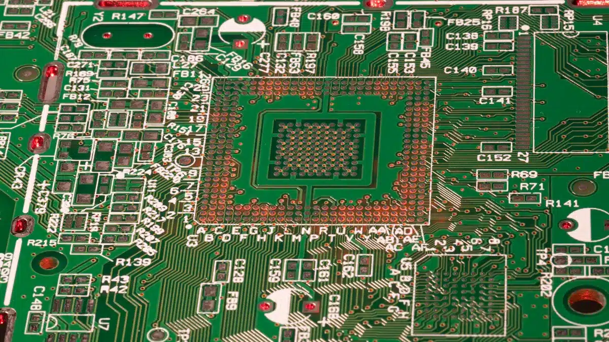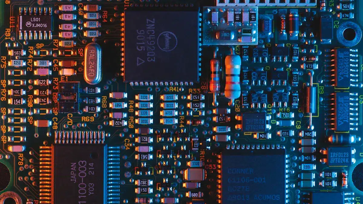
A printed circuit board, or PCB, is very important in electronics. Understanding the pcb board definition helps clarify its role in almost every electronic device you use, such as your smartphone or computer. A PCB is a flat board that holds parts of a circuit and connects these parts so they work together. Most modern electronics require a printed circuit board because it keeps all the components organized and in place. It also helps signals travel where they need to go. The way a PCB is made directly impacts how well devices perform and how long they last. When you look inside your favorite gadget, you’ll see the PCB, whose smart design is essential for the circuit to function properly.
Key Takeaways
A printed circuit board (PCB) holds and connects all electronic parts. It is the main support for things like smartphones and computers.
PCBs have many layers made from copper and FR-4. These layers help move signals, control heat, and protect circuits.
There are different PCB types—rigid, flexible, and rigid-flex. Each type fits different devices, like strong laptops or bendable wearables.
Good PCB design uses smart layer setups and careful part placement. This keeps signals clear, lowers noise, and helps control heat.
PCBs give electrical connections, support, and insulation. This helps devices work well and last longer.
PCB Board Definition
What Is a Printed Circuit Board
When you look at the inside of any electronic device, you will find a printed circuit board. The pcb board definition is simple. A printed circuit board is a flat board that connects and supports all the electronic parts in a device. You can think of it as the backbone of your gadget. The pcb board definition also includes the way it organizes and holds components like resistors, capacitors, and chips.
A printed circuit board uses copper pathways to let electricity and signals move between parts. These pathways follow a schematic, which is a special drawing that shows how everything connects. The schematic acts like a map for the pcb board definition. It helps you understand where each part goes and how signals travel. When you follow a schematic, you can see how the design of the pcb matches the needs of the device.
Tip: If you want to build your own electronic project, always start with a schematic. It will guide your pcb board definition and help you avoid mistakes.
Why Structure Matters
The structure of a pcb is very important. The pcb board definition is not just about holding parts. It is also about making sure the device works well and lasts a long time. The way you design the printed circuit board affects how signals move and how safe the device is.
Here are some key functions of a pcb board definition:
It connects all the parts a device needs, acting as a platform for electronic components.
It provides channels for electricity and signals, letting your device perform its tasks.
It supports mounting of both simple and complex parts, from resistors to microchips.
It allows for efficient and automated manufacturing, making devices more reliable.
A good schematic helps you plan the design. When you follow the schematic, you make sure each part sits in the right place. The pcb board definition always depends on the schematic and the design choices you make. If you want your device to work well, pay close attention to the schematic and the structure of your pcb.
Structure of a Printed Circuit Board

Layers and Materials
When you look at a pcb, you see more than a flat board. The pcb structure is like a sandwich with many layers. Each layer does something special. Most stack-ups have copper foil, insulation, and sometimes prepreg. Prepreg is a sticky fiberglass sheet that holds layers together.
Each layer uses different materials. The table below lists common materials and their features:
Material | Dielectric Constant (Dk) | Loss Tangent (Df) | Thermal Conductivity (W/m·K) | Glass Transition Temp (Tg, °C) | Typical Applications |
|---|---|---|---|---|---|
FR-4 (Glass Epoxy) | ~4.0 | ~0.02 | ~0.3-0.4 | 130-180 | General-purpose PCBs, low-cost electronics |
Rogers Laminates | ~3.48 | ~0.002 | ~0.6 | N/A | RF/microwave, high-frequency digital |
Polyimide (PI) | ~3.5-4.0 | ~0.01-0.02 | ~0.2-0.4 | 250-260 | Flexible PCBs, high-temperature applications |
PTFE (Teflon) | ~2.2-2.5 | 0.0005-0.005 | ~0.2 (pure), ~0.5 (filled) | N/A | RF/microwave circuits, high-frequency apps |
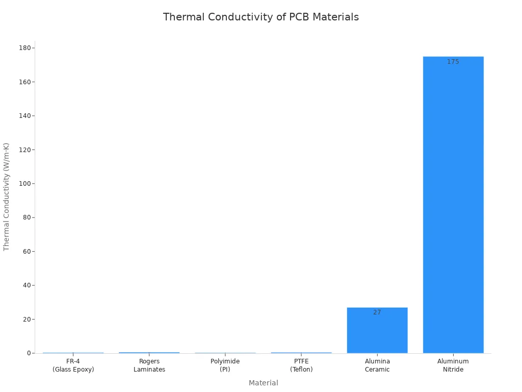
Alumina Ceramic (Al2O3) | ~9.8 | ~0.0001 | 24-30 | >300 | High-power LEDs, RF power modules |
Aluminum Nitride (AlN) | ~8.8 | ~0.0001 | 150-200 | >300 | High-performance power electronics, military |
Liquid Crystal Polymer | ~3.0 | Very low | Not specified | Up to ~200 | High-frequency flexible circuits, 5G antennas |
Composite Epoxy Material (CEM) | Higher than FR-4 | Higher than FR-4 | Not specified | Not specified | Low-cost, simple single-layer boards |
The material you pick changes how your pcb works. FR-4 is used most because it is cheap and strong. Rogers and PTFE are better for high-frequency circuits. Polyimide lets the board bend, so it is good for flexible electronics. Ceramics handle heat well, so they are used in power devices.
You can see how each material handles heat in this chart:

The number of layers in a pcb matters a lot. More layers let you fit more circuits and help signals stay clear. You get less noise and better power. But more layers make the pcb thicker and cost more. Simple devices use one or two layers. Complex electronics use four, six, or even more layers.
Note: Picking the right stack-up and materials is important for pcb design. It changes how fast signals move and how heat is controlled.
Copper Traces and Pads
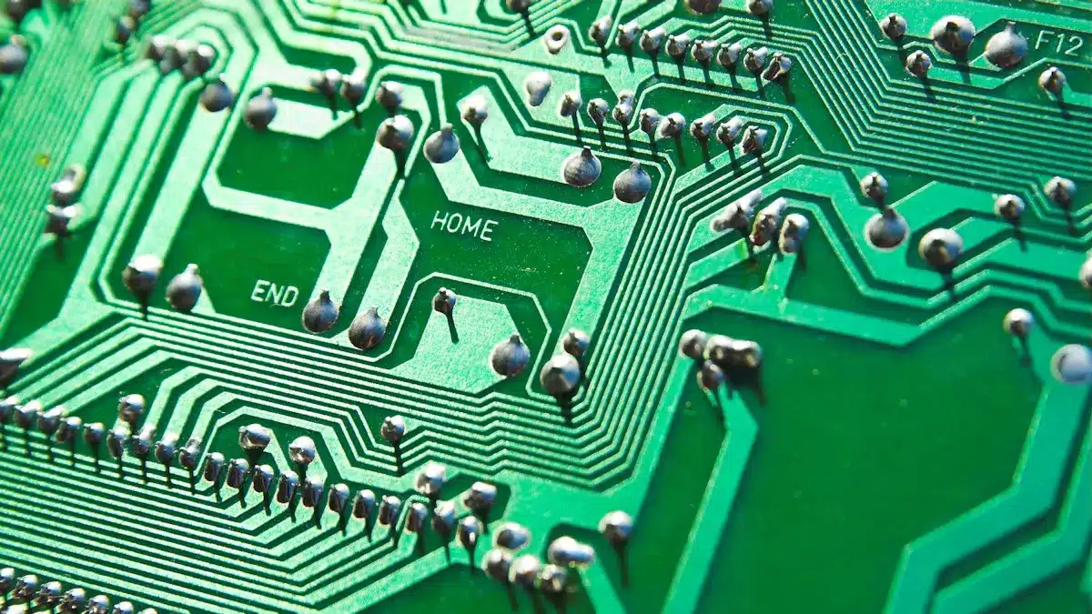
Copper traces are like tiny roads for electricity. They connect all the parts on your pcb. You find traces on every layer. The width and thickness of a trace decide how much current it can carry. Thicker traces carry more current and stay cooler. Most pcbs use copper that is 1 oz/ft² thick, but high-power circuits use thicker copper.
How you lay out traces keeps signals clear and stops overheating. If traces are too thin, they can burn out or cause problems. The stack-up lets you put traces on different layers. This helps you route signals without crossing over.
Copper pads are spots where you attach parts. Pads come in many shapes and sizes. Through-hole pads let you put leads through the board. Surface-mount pads hold parts on top. Pads make soldering easy and keep parts in place. They also help move heat away from hot parts.
Copper pads and traces work together to connect, support, and cool your parts. Good pad design means strong solder and reliable circuits.
Substrate and Insulation
The substrate is the main base layer in your pcb. It gives the board its shape and strength. FR-4 is the most used substrate. It is strong, cheap, and insulates well. Some boards use metal or ceramic substrates for better heat control. Flexible substrates, like polyimide, let you bend the pcb for special uses.
Description | Advantages | |
|---|---|---|
FR4 | Composite of woven glass fibers and epoxy resin, widely used for general PCB applications. | Excellent electrical insulation, high mechanical strength, cost-effective, versatile for many uses. |
Insulated Metal Substrate (IMS) | Metal core (aluminum/copper) with thermally conductive insulating layer for heat dissipation. | Superior heat dissipation, reduces overheating risk, ideal for power electronics and LED lighting. |
Ceramic Substrates | Materials like Aluminum Nitride and Silicon Nitride for high-performance, extreme conditions. | High thermal conductivity and resistance, suitable for high-frequency and high-temperature applications. |
Flexible Substrates | Made from Polyimide or Polyester, allowing bending and folding. | Lightweight, flexible, durable; ideal for wearable electronics, medical devices, and compact designs. |
High-Frequency Materials | Examples include Rogers 4003c, designed for microwave and radio frequency applications. | Low dielectric loss, stable dielectric constant, maintains signal integrity at high frequencies. |
Insulation sits between copper layers in the stack-up. It keeps electricity from jumping between traces or layers. This stops shorts and keeps your circuits safe. Insulation also helps with heat and makes the pcb strong. Good insulation means your pcb lasts longer and works better.
Insulation stops unwanted current and keeps signals clear.
It protects against heat and stops warping.
It supports the whole pcb, so your board stays strong.
Insulation is just as important as copper in your pcb. Without it, your circuits would not last long.
PCB Design and Layout

Layer Arrangements
When you design a pcb, you must plan the layers. The stack-up is the order of these layers. A good stack-up helps your board work well and last longer. It controls how signals move and how noise is handled. If you put a ground layer next to a signal layer, signals stay clean. This also lowers interference and makes your device work better.
A smart stack-up helps with power too. Power and ground layers act like shields. They protect your circuit from outside noise. You can see common layer setups in this table:
PCB Type | Layer Arrangement Description | Typical Materials and Features |
|---|---|---|
Single-layer | One copper layer on one side of the board. Parts go on one side only. | FR-4 or phenolic resin; Copper is 18-35μm thick; Solder mask and silkscreen on top only. |
Double-layer | Copper on both sides, connected by vias. Parts can go on both sides. | FR-4 with good stability; Copper is 18-35μm or thicker; Solder mask and silkscreen on both sides; Special finishes possible. |
Multilayer | Many copper and insulation layers pressed together. Inside layers are often for power and ground. | Laminated fiberglass epoxy; Usually 4, 6, 8 or more layers; Layers are arranged for best routing, shielding, and signal quality. |
Tip: Add a ground layer to your stack-up. This helps signals stay clear and reduces noise.
Single, Double, and Multi-Layer PCBs
You pick single, double, or multi-layer boards for your needs. Single-layer pcbs are simple and cheap. They are used in things like calculators. Double-layer boards give more room for parts and better wiring. You find them in wearables and medical tools. Multi-layer pcbs have three or more layers. They are used for complex designs and better performance. These are found in smartphones and airplanes.
Multi-layer boards let you keep power, ground, and signal layers apart. This keeps signals strong and cuts down on interference. Multi-layer pcb design also makes devices tougher and more reliable.
Component Placement
Where you put parts on the pcb is very important. Good placement helps heat move away and keeps signals short. Put hot parts near heat sinks or thermal vias to cool them. Leave space between high-power parts to stop hot spots. Use thermal vias to move heat to other layers. Good placement keeps solder joints strong and stops damage from heat.
When you plan your layout, use computer tools to test heat and signals. These tools help you find problems before making the board. Always follow your schematic so each part is in the right spot. Careful design and layout make your circuit safe, strong, and work well.
Types of PCBs
Rigid and Flexible PCBs
There are different types of pcb boards in electronics. The main types are rigid, flexible, and rigid-flex. Rigid pcbs are hard and do not bend at all. You see rigid boards in things like laptops and game consoles. These boards hold all the parts steady and safe. Flexible pcbs are made from materials that can bend and twist. Polyimide is a common material for flexible boards. You find flexible boards in wearables and foldable gadgets. Rigid-flex pcbs mix both types in one board. They give you both strength and flexibility. This helps when a device needs to fit in small spaces or move a lot.
PCB Type | Description | Common Uses |
|---|---|---|
Rigid | Solid, inflexible, strong support | Smartphones, laptops, industrial controls |
Flexible | Bendable, lightweight, fits tight spaces | Wearables, medical devices, foldable phones |
Rigid-Flex | Mix of rigid and flexible sections | Cameras, aerospace, military equipment |
Tip: Flexible pcbs are better for bending and shaking. They work well in devices that move or have odd shapes.
HDI and Advanced Types
High density interconnect pcbs are used in many new devices. These boards have tiny holes and thin lines. They let you put more parts in a small space. This makes devices work faster and better. HDI boards use lasers to make very small holes. These holes help control heat and signals. You can use fewer layers and still get great results.
You find high density interconnect pcbs in tablets and fast computers. They are also in medical and space equipment. These boards help make devices smaller and lighter. High density interconnect boards use special vias that only connect some layers. This keeps the board thin and strong.
Here is a quick comparison:
Feature | HDI PCB | Traditional PCB |
|---|---|---|
Component Density | Very high | Lower |
Board Size | Smaller, lighter | Larger, heavier |
Via Technology | Microvias, blind/buried vias | Through-hole vias |
Signal Integrity | Excellent | Good |
Applications | Smartphones, wearables, servers | Radios, basic appliances |
High density interconnect pcbs use stacked vias and thin traces.
They give better signals and less noise.
HDI boards save power and last longer.
Note: High density interconnect technology is important for new electronics. It lets you make smaller and faster devices with HDI pcbs.
PCB Functions
Electrical Connectivity
A pcb connects all the parts in your device. Copper traces act like tiny roads for signals and power. These traces link microchips, resistors, capacitors, and connectors. Together, they make a full circuit. When you use a smartphone, the CPU talks to memory chips through these copper lines. The pcb lets signals move between microchips. This allows data to be shared and saved. Good connections help your device work right. There are single-sided, double-sided, and multi-layer pcbs. Each type supports different circuit sizes and designs. You see them in simple radios and advanced computers. The pcb design keeps signals strong by controlling impedance and using ground planes. This makes your circuits work well and stops interference.
PCB Type | Characteristics | Typical Applications |
|---|---|---|
Single-sided PCBs | Conductive traces on one side; simple and cost-effective | Calculators, radios, LED lights |
Double-sided PCBs | Conductive traces on both sides; supports higher component density | Mobile phones, printers, routers, modems |
Multi-layer PCBs | Three or more layers of conductive traces separated by insulation; high circuit density and performance | Computers, laptops, server motherboards, advanced medical equipment |
Mechanical Support
A pcb gives strong support for all the parts in your device. It holds microchips and other pieces in place. The board has layers with insulation between copper. This keeps everything steady and safe. Through-hole parts make the board even stronger. The pcb fits inside your device and protects the circuit from shaking. Rigid boards use fiberglass for strength. Flexible boards use polyimide so they can bend. Rigid-flex boards mix both types for special shapes and folding. This support keeps your circuit safe, even in hard conditions.
PCB Type | Structural Material | Contribution to Physical Durability |
|---|---|---|
Rigid PCB | Solid fiberglass (FR4) | Retains shape, provides a stable and robust platform for components |
Flexible PCB | Bendable materials (polyimide) | Allows bending/flexing while maintaining durability |
Rigid-Flex PCB | Combination of rigid and flexible materials | Offers both stability and flexibility for devices requiring folding |
Metal-Core PCB | Metal base (often aluminum) | Enhances heat dissipation and durability under thermal stress |
Tip: Through-hole mounting makes your board stronger, especially for heavy parts.
Insulation and Protection
Insulation keeps your circuit safe from harm. The pcb uses FR-4, polyimide, and ceramic to separate copper layers. This stops short circuits and keeps parts safe. Insulation protects against heat, water, dust, and rust. Special coatings cover the board to block moisture and chemicals. These coatings stop rust and keep copper traces safe. Good insulation and coatings help your board last longer. They also keep your circuit working well. Insulation helps your board handle heat and shaking, which is important in planes and defense gear.
Insulation Material | Key Properties and Applications |
|---|---|
FR-4 | Fiberglass reinforced epoxy laminate; flame retardant; good electrical insulation; high temperature resistance; cost-effective. |
Polyimide | High temperature tolerance (up to 400°C); excellent mechanical and electrical properties; ideal for high-temp applications. |
Teflon (PTFE) | Non-conductive; excellent electrical and thermal insulation; low dielectric constant; suited for high-frequency PCBs. |
Ceramic | Excellent electrical properties; low dielectric constant; suitable for high-frequency and high-speed applications. |
Radio Frequency | Enables high radio frequency operation; ideal for aerospace applications to maintain signal integrity. |
Metal | Metals like copper and aluminum used for heat resistance and effective current flow; used in high current PCBs. |
Note: Protective coatings help your pcb last longer and stop rust, keeping your circuits and microchips safe.
You can see how the PCB board’s structure helps devices work. Copper traces, layers, and materials connect and protect parts. They also give support to all the electronic pieces. If you learn about PCB design, you can find and fix problems faster. Look inside things like phones or game consoles to spot a PCB.
Rigid, flexible, and metal-core PCBs have special uses.
If you want to know more, check out guides on PCB design, making, and testing from trusted sources. 🛠️
FAQ
What does PCB stand for?
PCB stands for “Printed Circuit Board.” You see PCBs in almost every electronic device. They connect and support all the electronic parts so your device works properly.
Why do PCBs use copper?
You find copper on PCBs because it conducts electricity very well. Copper traces let signals and power move quickly between parts. This helps your device run smoothly.
Can you repair a damaged PCB?
Yes, you can repair some PCB problems. You might fix broken traces with solder or special wire. If the damage is too big, you may need to replace the board.
How do you clean a PCB safely?
Use a soft brush and isopropyl alcohol to clean your PCB. Make sure you unplug the device first. Let the board dry completely before turning it on again.
What is the difference between single-layer and multi-layer PCBs?
Type | Layers | Use Case Example |
|---|---|---|
Single-layer | 1 | Simple toys, calculators |
Multi-layer | 3+ | Computers, smartphones |
Multi-layer PCBs handle more parts and signals. Single-layer boards work for simple devices.
See Also
Understanding Key Functional And Structural Variations Of PCBA And PCB
Essential PCBA Parts And Their Primary Roles Explained Clearly
Unveiling The Lesser-Known Contrasts Between PCBA And PCB
A Deep Dive Into PCBA Testing Methods For Modern Electronics
Defining PCBA And Highlighting Its Major Uses In Electronics