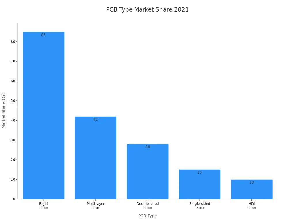
Electronics designers have many choices when it comes to printed circuit board production. Most devices use rigid PCBs, which make up 85% of the market. Rigid PCBs are strong and versatile, making them useful in many applications. The process of printed circuit board production involves two main steps. First is fabrication, which builds the board itself. Second is assembly, where parts are placed on the board. Flexible printed circuit boards are becoming increasingly popular, especially in wearables and medical devices, and this segment is growing rapidly. Key factors such as cost, production speed, and manufacturing complexity play a significant role in printed circuit board production. Additionally, material waste and quality control impact every stage of making printed circuit boards.
PCB Type | Market Share (2021) | Notes on Usage and Trends |
|---|---|---|
Rigid PCBs | 85% | Used most because they are strong and useful. |
Multi-layer PCBs | 42% | Used for hard and high-performance devices. |
Double-sided PCBs | 28% | Found in many electronics, not too hard to make. |
Single-sided PCBs | 15% | Used for simple things, easy circuits. |
HDI PCBs | 10% | High-density, found in phones and wearables; cost more but are important. |
Flexible PCBs | N/A (forecast $41B by 2030) | Growing fast, used in wearables and medical electronics. |
Key Takeaways
Rigid PCBs are tough and cheap. They are used in many gadgets. Flexible PCBs can bend and fit into tight spots. They work well in wearables.
There are different ways to make PCBs. Subtractive, additive, and laser direct imaging are some methods. Each method has its own cost, speed, and design benefits.
There are different ways to put parts on PCBs. Through-hole and surface mount are two main types. These affect how big, strong, and fast devices are made.
Quality control is very important for PCBs. Automated checks and tests help make sure PCBs work right. They also help meet high standards.
Picking the best PCB method is important. It depends on what the device needs, cost, how many are made, design limits, and what the factory can do. This helps save money and time.
PCB Manufacturing Methods
Rigid PCB
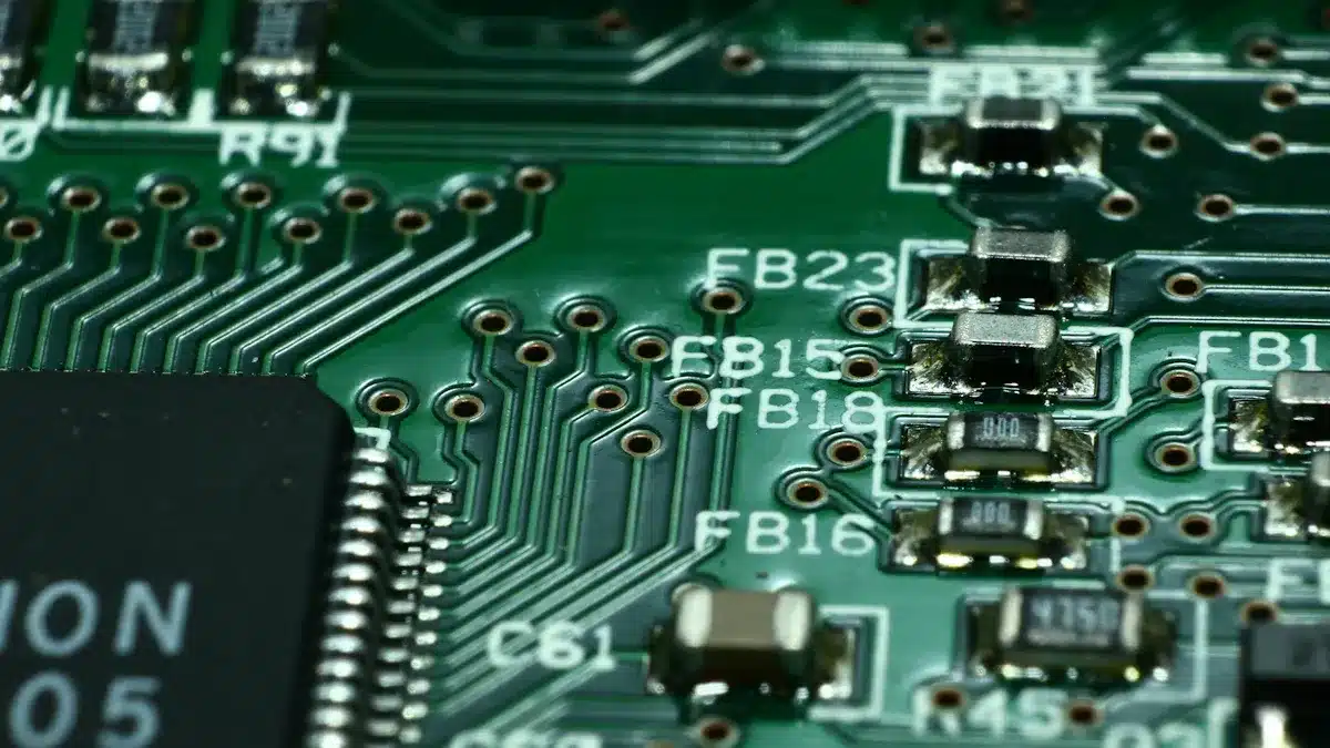
Rigid PCBs are used in most electronics. They have a hard base that does not bend. This makes them strong and able to hold many parts. You can find rigid PCBs in computers, phones, TVs, and machines. They work well in hot places and last a long time. Medical tools like pacemakers use them because they are exact and tough. Planes and military gear also use rigid PCBs for their strength. Making rigid PCBs means putting copper and a solder mask on a solid board. This way is cheaper and easier, especially for boards with many layers.
Rigid PCBs are strong, handle heat, and cost less for big jobs.
Flexible PCB
Flexible PCBs have a soft base like polyimide. This lets them bend, twist, and fit in small spaces. They are lighter and thinner than rigid PCBs. People use flexible PCBs in phones, smart watches, medical tools, and cars. These boards can take the place of wires, so there is less waste. Flexible PCBs keep working even if they move or shake. To make them, copper is rolled onto the bendy base and covered for safety. This helps make small and creative products.
Rigid PCB | Flexible PCB | |
|---|---|---|
Substrate Material | Hard, does not bend, often glass inside | Soft base like polyimide |
Flexibility | Stays stiff | Can bend and twist |
Conductive Material | Copper put on by electricity | Copper rolled on (bends more) |
Protective Layer | Solder mask | Coverlay (protective layer) |
Typical Applications | Big things like TVs and computers | Small things like phones and wearables |
Thermal Resistance | Handles heat well | Handles heat and shaking |
Cost | Usually costs less | Usually costs more, but saves space |
Rigid-Flex PCB
Rigid-flex PCBs mix hard and bendy parts in one board. This lets products bend and twist but still stay strong. Rigid-flex PCBs save space and weight by not needing extra parts. They are easier to put together and break less often. Doctors, car makers, plane builders, and tech companies use rigid-flex PCBs for special needs. These boards can be made in many shapes and hold lots of parts. Making rigid-flex PCBs needs careful steps and good handling. Special things like ZIF tails, hidden holes, and air gaps help make cool designs and fit more in less space.
Rigid-flex PCBs let you make boards that bend and stay strong, perfect for tricky devices.
PCB Manufacturing Techniques
Modern electronics need different pcb manufacturing techniques to make good boards. Each way has special steps and works best with certain materials or board types. Knowing these ways helps designers pick the best one for their project.
Subtractive Process
The subtractive process is a very common pcb manufacturing technique. This way takes away extra copper from a board to make the circuit shape. The steps are:
Use a board covered with copper.
Put a photoresist layer on the copper.
Shine UV light through a patterned film to harden the photoresist in some spots.
Use chemicals to remove copper that is not protected.
Take off the photoresist to show the copper lines.
Add finishes to keep the copper safe and help with soldering.
This way works for both rigid and flexible pcb types. It is good for making lots of boards and helps keep quality high.
Additive Process
The additive process puts copper only where it is needed. It does not take copper away. This way uses less material and makes less waste than the subtractive process. Additive pcb manufacturing techniques are better for the environment and can help lower harm to nature. They also make boards thinner and lighter, which is important for flexible electronics.
Aspect | Additive Process | Subtractive Process |
|---|---|---|
Minimal waste | More waste | |
Environmental Impact | Lower | Higher |
Board Types | Flexible, Rigid, Rigid-Flex | Rigid, Flexible |
Laser Direct Imaging
Laser direct imaging (LDI) uses a laser to draw the circuit pattern right onto the photoresist. This way does not need a mask, so it saves time and makes fewer mistakes. LDI is very exact and can make lines as small as 5 microns. It lets people change designs fast, so it is great for testing and small batches. LDI works well for high-density interconnect (HDI) boards and helps line up layers better.
LDI gives clearer images, better matching, and less waste than old ways.
Pattern Plating
Pattern plating is another key pcb manufacturing technique. In this way, copper is put only on the spots marked by the photoresist pattern. This method is good for making tiny features and is often used with HDI boards. Pattern plating works for both rigid and flexible pcb types and helps make boards with lots of circuits.
These pcb manufacturing techniques give engineers many choices to fit their design, material, and how many boards they need.
PCB Assembly Methods
Printed circuit board assembly methods decide how devices work and look. Each way has special benefits for putting parts on the board and fitting many parts close together.
Through-Hole Technology
Through-hole technology uses parts with leads that go through holes. Workers or machines solder these leads on the other side. This makes strong bonds, so it is good for parts that get pushed or pulled, like connectors and transformers. Military and aerospace groups like through-hole technology because it is very reliable. Big parts need more space, so you cannot fit as many on the board. Making these boards takes longer and needs more work because you must drill and solder on both sides.
Through-hole technology is strong and lasts long, but it uses more space and takes more time to make.
Aspect | Through-Hole Technology (THT) | Surface Mount Technology (SMT) |
|---|---|---|
Component Attachment | Leads in drilled holes | Mounted on PCB surface |
Mechanical Strength | Strong bond | More fragile |
Component Size & Density | Larger, lower density | Smaller, higher density |
Assembly Process | Slower, labor-intensive | Faster, automated |
Suitability | Stress, durability needs | Miniaturized electronics |
Surface Mount Technology
Surface mount technology puts parts right onto the pcb surface. You do not need holes, so you save space and can fit more parts. Machines use solder paste and ovens to attach parts fast. Designers pick surface mount technology for small devices and circuits that need to work at high speeds. The parts are smaller and break easier, so checking and fixing them is harder. Most new electronics use this way because it is faster and fits more parts in less space.
Surface mount technology helps make things faster and smaller, but the parts may not handle heat as well.
HDI Technology
High-density interconnect (HDI) technology lets boards hold even more parts by using tiny holes and thin lines. HDI boards fit lots of parts in small spaces, so you get higher density. Makers use special materials and lasers to make tiny holes and fine lines. HDI technology lets you put parts on both sides of the board, so you need fewer layers and get better performance. Shorter spaces between parts help signals and save power. HDI technology makes small, light boards for phones, tablets, and wearables.
HDI boards use microvias and via-in-pad to put parts closer together.
Special materials help make thinner lines and smaller holes.
Ways like sequential lamination make boards stronger and help with heat.
HDI technology lets you do more with fewer layers by combining functions.
HDI technology gives higher circuit density and better performance, so it is important for modern, small electronics.
Printed Circuit Board Production Stages
Making printed circuit boards has many steps. Each step helps make sure the board works well. Every stage shapes the board and checks if it meets the plan.
Inner Layer Fabrication
Engineers begin with inner layer fabrication. They use CAD and CAM software to design the circuit. The base gets covered with copper. A photoresist is put on top. Ultraviolet light shows the pattern. Chemicals wash away extra copper. This makes the circuit lines on the inside layers.
Lamination
Lamination sticks layers together. Workers stack inner layers, prepreg, and copper foil. Heat and pressure glue them into one board. Sometimes problems like blistering or delamination happen. Clean rooms and good materials help stop defects. Vacuum lamination also helps. Engineers use pins and careful heating to keep layers lined up.
Tip: Pick materials that expand the same amount with heat. This stops stress and keeps the board from bending during lamination.
Drilling and Plating
Drilling makes holes for parts and connections. Machines drill exact holes through the board. Metallization coats the hole walls with copper. Copper plating makes strong links between layers. Good drilling and plating are needed for boards to work well.
Image Transfer
Image transfer sets the circuit shape on the outside layers. Workers put on photoresist and shine light through a mask. Chemicals take away copper that is not covered. This leaves the right circuit paths. The board is now ready for assembly.
Solder Mask and Surface Finish
Solder mask protects the board and stops solder bridges. Workers add a green or colored layer, leaving pads open. Surface finish like HASL or ENIG covers the pads. This helps solder stick and stops rust. These coatings keep the board good during assembly and use.
Routing and Testing
Routing cuts the board to its final size. Engineers use machines to separate each pcb from the panel. Testing looks for faults and defects. AOI, X-ray, and thermal imaging find problems without hurting the board. These tests make sure every pcb is high quality before assembly.
Stage | Purpose |
|---|---|
Inner Layer Fabrication | Make circuit lines on inside layers |
Lamination | Glue layers into one solid board |
Drilling and Plating | Drill holes and make electrical links |
Image Transfer | Set circuit shape on outside layers |
Solder Mask & Finish | Protect lines and help solder stick |
Routing and Testing | Cut boards and check for problems |
These steps help make boards ready for adding parts and final assembly.
Comparative Analysis
Cost
Cost is very important when picking pcb manufacturing methods. Setup costs matter most for small batches. Manufacturers pay a lot for tools and masks. These costs get split over a few boards, so each one costs more. When you make more boards, setup costs get shared. Automation helps lower labor costs in big batches. Advanced methods like HDI technology or heavy copper plating cost extra. This makes small batches even more expensive.
Production Volume | Setup Costs Impact | Per-Unit Cost Example (4-layer PCB) | Cost Drivers |
|---|---|---|---|
Low Volume (e.g., 10 units) | Setup costs are high (e.g., $100-$500 per design) | About $10 per board | Tooling and mask costs are spread over a few boards |
Medium Volume (e.g., 100-1,000 units) | Setup costs are shared over more boards | About $2-$5 per board | Per-board setup cost goes down, some savings |
High Volume (e.g., 10,000+ units) | Setup costs are very low per board (e.g., $0.05 per board) | Less than $2 per board | Big savings, automation cuts labor by 10-15% |
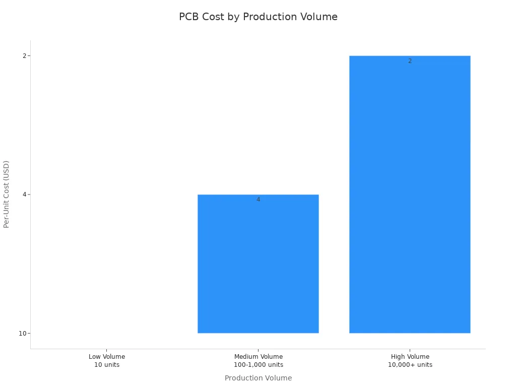
Advanced pcb manufacturing methods cost more, especially for tricky designs and small batches.
Production Speed
Production speed changes with the method and board type. Subtractive processes are fast for simple boards. Additive processes take longer for detailed patterns but help with testing. Laser direct imaging makes things quicker by skipping masks. HDI technology uses machines to build boards faster, especially for packed designs. Asian factories finish big orders quickly because their steps are smooth.
Subtractive techniques: Quick for easy boards, slower for complex ones.
Additive techniques: Good for testing and small batches, slower for lots of boards.
Laser direct imaging: Makes changes fast and cuts setup time.
HDI technology: Uses machines for quick building of packed boards.
Design Complexity
Hard designs need advanced pcb manufacturing methods. Things like plated edges, castellated holes, and cavity boards need special stuff and exact machines. Cavity boards use certain prepreg to stop dirt. Tight rules make things harder and cost more. Plated edges and castellated holes need extra plating and special drilling. These steps take more time and need special setups. Hard routing and plating mean more film swaps and machine changes. When designs get harder, makers use advanced ways like additive manufacturing or 3-D printing. These ways handle tiny details and tight rules better than old methods.
Makers must balance cost, time, and how well things work for hard designs. Advanced ways help meet design needs and keep costs down.
Material Waste
Material waste is different for subtractive and additive pcb manufacturing techniques.
Additive manufacturing puts copper only where needed, so less waste.
Subtractive manufacturing takes away extra copper, making waste chips even if recycled.
Additive ways lower material costs and waste removal bills.
Subtractive ways use more chemicals and power, which hurts the environment.
Additive techniques help save materials and are better for nature.
Additive pcb manufacturing methods save materials and help the planet, especially for hard designs.
Circuit Density
Circuit density means how many circuits fit on a board. HDI technology makes boards denser by using microvias, blind and buried vias, and laser drilling. These ways let makers use thinner lines and smaller holes. Sequential lamination stacks layers without making boards thick. Packed designs need careful planning and smart manufacturing.
Via choices change how well boards work and how packed they are, especially under BGAs.
Line width and space must match what makers can do and what designs need.
Closer lines make boards denser but can cause more mistakes.
Good design steps help make boards dense and reliable.
HDI pcb manufacturing methods help make small, packed circuits for new electronics. Makers use smart ways to shrink boards and make them work better.
Quality Control
Quality control makes sure pcb production is good, especially for packed and hard designs. Makers use many steps to keep quality high.
Picking the right materials stops solder problems and bad connections.
Good pcb design avoids trouble by setting the right wire width, space, and heat control.
Steady steps in drilling, plating, etching, and finishing stop mistakes.
Smart testing and checking during building find problems early.
Quality control steps include:
Automated Optical Inspection (AOI): Finds visual mistakes like parts in the wrong spot and bad solder.
X-ray Inspection: Finds hidden solder problems under BGAs.
Solder Paste Inspection (SPI): Checks solder paste amount and spot before adding parts.
In-Circuit Testing (ICT) and Functional Testing: Checks if circuits work and devices run right.
Process Traceability: Tracks making and checking steps for review and rules.
Statistical Process Control (SPC): Watches data to stop mistakes.
Employee Training: Makes sure workers know how to keep quality high.
Environmental Stress Screening (ESS): Tests boards with heat and shaking to find hidden problems.
Good quality control uses smart design, careful making, and strong checking to make sure pcbs work well.
Choosing the Right PCB Manufacturing Method
Picking the best way to make a printed circuit board depends on many things. Each project is different and has its own needs. Engineers must think about what the board must do, how much it costs, how many boards are needed, design limits, and what the factory can handle. Making a good choice saves money, gets boards made faster, and keeps quality high.
Technical Needs
Every project starts with what the board must do. Engineers decide how the board will work in the device. Some electronics need special machines to make them. Machines like pick-and-place, solder paste printers, and reflow ovens help make boards very exact. Checking quality is very important. Factories should follow rules like ISO 9001, IPC-A-610, or AS9100 for planes. Testing in the factory, like functional and in-circuit tests, checks if the board works right.
Key Considerations | |
|---|---|
Reasonable Design | Layout, size, circuit stability, anti-interference, speed, line width, pad size |
Material Selection | Substrate (FR-4, aluminum, ceramic), conductive layers (copper, silver), solder mask |
Processing Technology | Printing accuracy, etching timing, drilling accuracy, soldering temperature |
Equipment Conditions | Equipment accuracy, stability, automation level |
Quality Control | Inspection at key steps, functional and reliability testing, standards compliance |
Engineers follow careful steps to make the board. They finish the design, pick the right board, make circuit lines with chemical etching, put on photo-resist, drill holes carefully, and add solder mask for safety. Every step needs to be done right and at the right time. These steps help the board work for small and complex designs.
Tip: Always check if the factory can meet your project’s needs before you start making boards.
Cost Factors
Cost is important in every step of pcb manufacturing. Engineers look at the price for each board and the total project cost. Setup costs are high if you only make a few boards. Making more boards helps spread out these costs. Special ways to make hard designs, like HDI or special finishes, cost more. The materials you pick also change the price. Using normal materials like FR-4 keeps costs down. Special materials like ceramics or aluminum cost more.
Cost Factor | Impact on Project |
|---|---|
Setup Costs | Higher for small batches |
Material Choice | Standard is cheaper |
Advanced Features | Raise costs for complex designs |
Automation Level | Lowers cost for large volumes |
Engineers should ask for clear prices. They should check if the price covers testing, setup, and delivery. Saving money is good, but quality and delivery time matter too.
Volume Requirements
How many boards you need changes how they are made. For a few boards or test boards, hand assembly works best. It is flexible and keeps costs low. Hand assembly is good for simple boards and projects that change a lot. For lots of boards, machines are better. Machines work fast and make every board the same. Using machines costs more at first, but saves money when making many boards.
Machine assembly is best for big batches and hard designs.
Flexible machines help with medium batches and changing needs.
Fixed machines are best for making lots of the same board.
Note: Picking the right way to put boards together helps finish on time and saves money.
Design Constraints
Design limits change how engineers make boards. Board size, thickness, and number of layers all matter. Small boards and more layers need special ways to make them. Making lines thinner and closer can lower the number of layers. Fewer layers mean less cost and easier making. Boards with many layers or special holes, like blind or buried vias, need HDI technology and careful planning.
Manufacturing Impact | |
|---|---|
Board Size Tolerance | Affects routing and scoring methods |
Board Thickness | Thicker boards need advanced processes |
Layer Count | More layers mean higher difficulty and cost |
Blind/Buried Vias | Require HDI technology and increase complexity |
How layers are stacked changes how well the board works. Multi-layer boards help signals and stop noise, but need special making. Engineers must balance how well the board works, cost, and how hard it is to make. Making designs easy to build helps avoid problems and keeps things running smoothly.
Manufacturer Capabilities
The right factory makes a big difference. Engineers must check if the factory can do what the project needs. For hard designs or big orders, the factory should have new machines and skilled workers. They should make boards for a good price, keep quality the same, and be able to make more if needed. Certifications like ISO 9001 or AS9100 show the factory meets high standards.
List what the project needs: layers, size, materials, number, time, and quality.
Check if the factory has new machines for drilling, plating, and testing.
Look for quality rules and testing like AOI and X-ray checks.
Ask about delivery times and if they can make boards fast.
Check the price, including setup and testing fees.
Good talking and tech help fix problems quickly.
Think about where the factory is for shipping and help.
Picking a factory with strong skills helps finish on time, stay on budget, and get good boards.
PCB manufacturing methods have different good and bad points. The table below shows how subtractive, additive, and laser direct imaging methods affect how products work:
Method | Best For | Limitation |
|---|---|---|
Subtractive Process | Saves money, used in many ways | Not as exact, makes more waste |
Additive Process | Makes tiny lines, high density | Hard to do, costs more |
Laser Direct Imaging | Good for testing, HDI boards | Costs a lot, slow for big jobs |
Engineers need to pick board materials and designs that fit the device. For most things, FR-4 works well. Polyimide is better when it gets very hot. In the future, electronics will get smaller. Flexible PCBs and green materials will become more important.
FAQ
What is the main difference between rigid and flexible PCBs?
Rigid PCBs are flat and do not bend. Flexible PCBs can bend and twist easily. Rigid PCBs are used in things like computers and TVs. Flexible PCBs are good for wearables and small gadgets.
Why do engineers choose HDI technology?
HDI technology helps fit more parts on tiny boards. This makes phones and smartwatches smaller and lighter. HDI also makes signals move faster and saves space.
How does the subtractive process work in PCB manufacturing?
The subtractive process uses a board covered with copper. Workers take away extra copper to make the circuit shape. This way works for many board types and costs less.
What quality control steps help ensure good PCBs?
Engineers use AOI, X-ray checks, and in-circuit tests. These steps find problems early and help every PCB work well.
Can PCB manufacturing methods affect the environment?
Method | Material Waste | Environmental Impact |
|---|---|---|
Additive | Low | Lower |
Subtractive | High | Higher |
Additive methods use less copper and fewer chemicals. Subtractive methods make more waste.
See Also
The Importance Of Custom PCBA In Today’s Electronics
Benefits And Obstacles Of Flex PCBA In Electronics
A Deep Dive Into PCBA Testing Methods For Electronics