
PCB prototype assembly means making a small number of circuit boards. This helps test and check if your design works well. It lets you find problems early and improve your product. This step is key for making sure your design works, is easy to make, and doesn’t cost too much.
Here are some benefits:
It tests heat, signals, and how it handles the environment.
It approves new parts and materials.
It makes sure it follows industry rules.
It lowers risks when moving to big production.
Prototyping is important for making a good and strong product.
Key Takeaways
PCB prototype assembly checks designs early to catch and fix errors.
Prototyping saves money by making production easier and avoiding costly changes.
Quick-turn services help products get made faster and reach markets sooner.
Working together during prototyping improves teamwork, creating better designs with fewer mistakes.
Following industry rules during prototyping ensures safety and quality, earning customer trust.
Purpose of PCB Prototype Assembly
Checking if the PCB design works
Testing your circuit board design is very important. It makes sure the PCB works before making many copies. Testing helps find mistakes that could cost a lot later. Fixing problems early makes your product more reliable.
For example, testing checks how the PCB handles signals, heat, and the environment. This step ensures the design works well and follows rules. Without testing, the product might not meet customer needs or pass regulations.
Finding and fixing design mistakes
Prototype assembly helps find and fix design mistakes early. During this phase, teams review designs and share ideas to improve them. Working together catches problems before they grow bigger.
Here’s a table showing how fixing mistakes reduces risks:
Benefit | Description |
|---|---|
Design Reviews | Regular checks improve designs and lower the chance of errors. |
Better Feedback | Teams share ideas to make the design stronger and safer. |
Team Collaboration | Different departments work together to spot hidden issues. |
Lower Technical Risks | Tests ensure parts work well and avoid failures. |
Following Rules | Early prototypes check if the design meets industry standards. |
Easier Manufacturing | Fixing problems early makes production smoother and faster. |
Fixing mistakes during prototyping saves money and makes production easier.
Making production easier and cheaper
Improving manufacturability during prototyping lowers costs and boosts efficiency. This step makes the design simpler and cheaper to produce. For example, you can try different materials or make assembly faster.
Here’s a table showing benefits of improving manufacturability:
Advantage | Description |
|---|---|
Avoiding Big Mistakes | Prototyping finds problems early, saving money later. |
Cheaper Materials | Tests allow using less expensive parts without losing quality. |
Removing Extra Features | Simplifies the design to save money and time. |
Prototyping also confirms the PCB works, speeding up production and market launch. This saves money and helps you sell your product faster.
Accelerating product development
Prototyping helps speed up making new products. By building a few circuit boards early, you can test and improve designs faster. This avoids delays caused by finding problems too late.
PCB prototyping allows quick changes to designs. You can test, get feedback, and fix issues quickly. For example, if a part causes signal problems, you can change the layout and test again. This process makes sure your final product works well.
It also helps try out new ideas or features. If you’re adding new technology, prototyping lets you test if it works. You can see how it fits with the design and make changes. This lowers risks and builds trust in your product.
Prototyping improves teamwork too. Engineers, designers, and makers can work better with a physical model. Everyone understands the design better, reducing confusion. This helps the project move faster and smoother.
Lastly, prototypes help meet tight schedules. Fixing problems early saves time and money. This lets you launch your product on time and stay ahead in the market.
Steps in the PCB Prototype Assembly Process
Preparing and reviewing design files
The first step is to prepare and check design files. This makes sure the prototype starts correctly. Good design files prevent mistakes and save time. Bad files can cause delays, extra costs, or product failures.
To avoid problems:
Check design rules to meet all limits.
Match component labels to avoid confusion during assembly.
Review designs with your team to find issues early.
Spending time on good data helps a lot. Skipping reviews can add 10-15% more time to projects. Each board fix might take 1-2 extra weeks. Costs can rise by 5-10% due to unclear files. Focusing on this step makes the next stages smoother.
Sourcing components and managing inventory
Getting parts and managing stock is very important. Without the right parts, your project may slow down or cost more.
Here are ways to improve:
Check needs to match stock with production.
Set reorder points to avoid running out.
Use just-in-time stock to save money.
Build trust with suppliers for better service.
Watch stock levels to reduce waste.
Strategy | How It Helps |
|---|---|
Checking needs | Matches stock with production needs |
Setting reorder points | Stops running out of parts |
Using just-in-time stock | Saves money and improves cash flow |
Building supplier trust | Makes delivery faster and more reliable |
Watching stock levels | Reduces waste and keeps stock at the right level |
These steps make the process easier and lower risks.
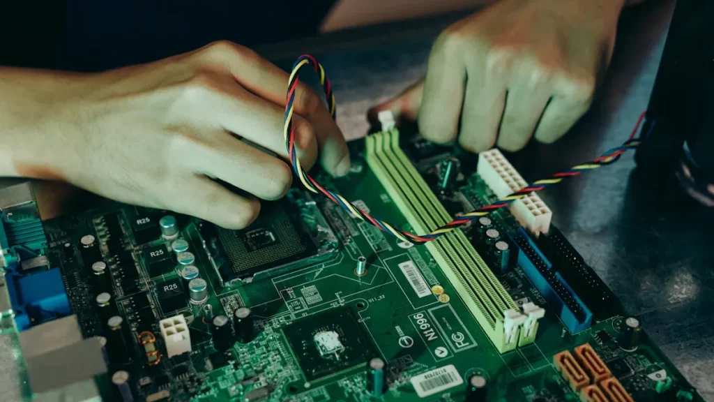
SMT pick-and-place assembly
SMT (Surface Mount Technology) pick-and-place is a key step. Machines place parts on the board with great accuracy. This step is important for making the board work well.
The machine reads the design and places parts as planned. This accuracy lowers mistakes and keeps track of parts. It’s very helpful for complex boards with tiny parts.
Step | What Happens |
|---|---|
Machines place parts on boards with high accuracy. | |
SMT Reflow Soldering | Boards are heated to attach parts permanently. |
Cleaning/Washing | Cleaning removes leftover flux after soldering. |
AOI and Functional Testing | Tests check if the board works and meets standards. |
Final Programming/Flashing | Software is added to test the board before shipping. |
This step improves quality and speeds up the process. Using SMT pick-and-place makes your prototype reliable and efficient.
Reflow soldering and through-hole soldering
Reflow soldering and through-hole soldering are key in making PCB prototypes. Each method helps ensure your PCB works well and lasts long.
In reflow soldering, solder paste is added to the PCB. Machines place parts on the board, which then goes through a reflow oven. The heat melts the solder, creating strong bonds. This method is common in gadgets like phones, tablets, and computers. It works best for small, detailed parts.
Through-hole soldering is different. It involves putting part leads into holes on the PCB. These leads are soldered to pads on the other side, often using wave soldering. This method is used in industrial machines and car electronics for large-scale soldering.
Each method has pros and cons:
Reflow soldering is great for small parts but struggles with big ones.
Through-hole soldering makes strong connections, good for heavy-duty uses.
Problems like weak solder or cracks can happen in both methods. But following proper standards can reduce these issues.
Tip: Pick the soldering method based on your PCB’s needs. Reflow soldering suits gadgets, while through-hole soldering fits industrial or car products.
Inspection and quality testing
Checking and testing are vital steps in making PCB prototypes. These steps make sure your PCB works as planned.
Different tests check if your PCB is reliable:
Test Type | Purpose | Criteria |
|---|---|---|
Automated Optical Inspection (AOI) | Pass/fail | |
Electrical Testing | Checks for circuit problems or wrong resistance. | Pass/fail |
Mechanical Testing | Tests the PCB’s physical strength. | Pass/fail |
Visual Inspection | Spots visible mistakes in the PCB. | Pass/fail |
Functional Testing | Confirms the PCB does its job correctly. | Pass/fail |
AOI uses cameras and software to find mistakes automatically. Electrical tests check if circuits work right. Mechanical tests ensure the PCB is strong. Visual checks find obvious flaws, and functional tests confirm the PCB works as it should.
Note: Testing during prototyping catches problems early. This saves time and money later.
Using these tests together ensures your PCB prototype is ready for production.
Benefits of PCB Prototype Assembly
Lowering risks in large production
Making prototype PCBs helps reduce risks in big production runs. Testing early finds and fixes problems before they become expensive. This step ensures your circuit board works well in real-life situations.
Prototypes are a cheap way to test and find mistakes.
Early checks stop costly redesigns or product recalls.
Prototypes reveal production issues, cutting down risks a lot.
For instance, if a mistake is found during prototyping, it can be fixed right away. Fixing problems early saves money and time while making your product better.
Speeding up product launch
Quick PCB prototyping makes product development faster. Using fast-turn PCB services helps test and improve designs quickly. This speed lets you release your product before competitors.
Business Type | Project Example | Result |
|---|---|---|
Tech Company | Made a health tracker with fast PCB prototyping. | |
Telecom Company | Built an advanced RF device using quick prototyping. | Successful launch with timely adjustments. |
Fast prototyping allows quick changes to meet market needs. For example, if a part doesn’t work well, you can replace it and retest fast. This flexibility ensures your product is ready for customers on time.
Improving designs step by step
Prototyping helps make your PCB design better with each try. Every version improves how it works, lasts, and is made. This process is key to creating a great product.
PCB prototyping lets you test new ideas and features. For example, you can try different materials or layouts to make the design better. Each prototype gives useful feedback to guide your choices.
Teamwork also gets better during prototyping. Engineers, designers, and makers can work together using a physical model. This reduces confusion and keeps everyone focused on the same goals.
Tip: Use prototypes to try new ideas and stay ahead in the market.
Ensuring compliance with standards
Meeting industry rules is very important for electronic products. PCB prototype assembly helps check if your design follows these rules. This step prevents failing tests and costly fixes later.
Standards like IPC, RoHS, and UL ensure safety and quality. During prototyping, you can test your PCB to meet these rules. For example, IPC checks solder quality and materials. RoHS ensures no harmful substances like lead are used. UL focuses on electrical safety.
Tip: Always check which rules apply to your product. This saves time and avoids problems later.
Here’s how prototyping helps meet standards:
Material Selection: Test materials to meet safety and environmental rules.
Design Validation: Check if your PCB layout follows design rules like spacing.
Functional Testing: Ensure your PCB works well under heat or vibration.
Documentation: Create records needed for certifications during prototyping.
Standard | Focus Area | Example Requirement |
|---|---|---|
IPC | Quality and reliability | Check solder joints |
RoHS | Environmental safety | No harmful materials like lead |
UL | Electrical safety | Test fire resistance and insulation |
By testing early, you lower the chance of breaking rules. This step also builds trust with customers and regulators. Following standards makes your product safer and ready for sale.
Note: Skipping compliance checks can cause delays, fines, or recalls. Always make this step a priority.
Types of PCB Prototype Assembly
Manual vs. Automated Assembly
When making a PCB prototype, you can pick manual or automated assembly. Manual assembly uses skilled workers to place and solder parts. It’s good for small projects and allows easy design changes. But it takes more time and may have human mistakes. Automated assembly uses machines for tasks like placing parts and soldering. It’s faster, more accurate, and better for large projects.
Here’s a simple comparison:
Aspect | Manual Assembly | Automated Assembly |
|---|---|---|
Advantages | Flexible for changes | Fast and precise |
Cheaper for small batches | Great for big productions | |
Skilled workers ensure quality | Consistent results | |
Challenges | Slow process | Hard to adjust quickly |
Mistakes from humans | Expensive setup | |
Needs more labor | Needs machine upkeep |
Tip: Use manual assembly for testing new designs. Choose automated assembly for repeated tasks.
SMT vs. Through-Hole Assembly
There are two main ways to assemble circuit boards: SMT and THT. SMT (Surface Mount Technology) places parts directly on the board’s surface. It’s great for small, light designs. THT (Through-Hole Technology) uses leads that go through holes in the board. This makes strong connections, perfect for tough environments.
Key differences include:
SMT makes smaller, lighter boards, saving 40-60% space and 60-90% weight.
SMT uses machines, making it faster and cheaper.
THT creates strong bonds, good for high-power or hot conditions.
Metric | SMT (Surface Mount Technology) | THT (Through-Hole Technology) |
|---|---|---|
High-Density Assembly | Small, lightweight designs | Bigger, less compact designs |
Efficient Automation | Fast, machine-based production | Slower, less automated |
Superior Electrical Performance | Better for high-frequency uses | Longer leads may lower performance |
Cost Reduction | Cheaper due to small parts | More expensive due to manual work |
Improved Reliability | Fewer defects | Stronger mechanical bonds |
Note: Pick SMT for modern gadgets. Use THT for industrial or car electronics.
Single-Layer vs. Multi-Layer Prototypes
Choosing between single-layer and multi-layer PCBs depends on your project. Single-layer PCBs have parts on one side. They’re simple, cheap, and good for basic devices like remotes. Multi-layer PCBs stack layers for complex designs like phones or medical tools.
Feature | Single-Layer PCB | Multi-Layer PCB |
|---|---|---|
Cost | Cheaper due to simple design | More expensive due to complexity |
Design Complexity | Best for simple devices | Needed for advanced gadgets |
Production Time | Faster to make | Takes longer to produce |
Application Suitability | Good for low-tech uses | Great for high-tech needs |
Size and Weight | Bigger and heavier | Smaller and lighter |
Durability | Less strong | More durable |
Tip: Use single-layer PCBs for simple tasks. Choose multi-layer PCBs for advanced, compact designs.
Factors Influencing Cost and Lead Time
PCB design complexity
How complex your PCB design is affects cost and time. Complicated designs need advanced tools, which cost more. Features like HDI or controlled impedance need precise work. This makes production harder and takes longer to finish.
Simple designs are quicker and cheaper to make. But, you must balance simplicity with how well it works. Knowing the trade-offs helps you plan your project better.
Tip: Keep your design simple but meet your product’s needs. This lowers costs and speeds up the pcb assembly process.
Component type and availability
The parts you pick and their availability affect cost and time. Special parts like BGAs cost more and need special tools. QFPs may cost less but can cause more errors, raising costs.
If parts are hard to find, your project may slow down. Picking good-quality parts avoids delays and reduces mistakes. Spending more on better parts can save money later by making the pcb assembly easier and error-free.
Note: Work with trusted suppliers to get parts on time. This keeps your project on schedule.
Prototype volume
How many prototypes you make affects costs. Small batches cost more per unit since they lack bulk savings. Scaling up can be tricky if your methods aren’t optimized.
Keeping your design the same in small runs can be hard. Changing manufacturers or methods might need adjustments, risking your design. Optimizing for small batches keeps costs low and quality high.
Tip: Plan your prototype numbers carefully to avoid extra costs and delays later.
Turnaround time requirements
Turnaround time is very important in PCB prototyping. It shows how fast you can test and improve designs. Faster turnaround helps meet deadlines and stay ahead in the market.
Making a PCB usually takes 2–8 weeks. Quick-turn services can make working PCBs in just 24 hours. For example, a simple 2-layer PCB might be done the same day. Complex ones, like an 8-layer PCB, may take 3–5 days. These services use faster methods and standard designs to save time.
Pick turnaround times based on your project’s needs. Quick-turn services are great for urgent projects. They let you test and fix designs quickly. Standard fabrication works better for projects with more time and lower costs.
Things that affect turnaround time include:
Design Complexity: Simple boards are faster. Complex ones need more testing and work.
Component Availability: Easy-to-find parts speed up production. Rare parts slow it down.
Volume of Prototypes: Small batches are quicker. Big orders take more setup and testing time.
Tip: Plan your schedule wisely. Use quick-turn for urgent needs and standard methods for flexible timelines.
Knowing turnaround time helps balance speed, cost, and quality. It keeps your PCB assembly process on track with your goals.
PCB prototype assembly is key to making good electronic products. It helps test designs, find mistakes, and make them better. Starting with small prototypes checks if the design works well. You can improve production step by step. Using methods like automated assembly saves money and keeps quality high. Testing tools like Automated Optical Inspection (AOI) check for problems early. This ensures your product is reliable without spending too much. Prototyping reduces risks and speeds up creating new products. It helps you launch smart ideas faster.
Tip: Focus on both quality and cost during prototyping for success.
FAQ
What is the purpose of PCB prototype assembly?
PCB prototype assembly lets you test your design early. It checks if your circuit board works, finds mistakes, and improves how it’s made. This step lowers risks and saves money by fixing problems before production.
How long does PCB prototype assembly take?
The time depends on your design and service choice. Simple prototypes might take a few days. Complex ones could take weeks. Quick-turn services can deliver in just 24 hours.
Can I use manual assembly for prototypes?
Yes, manual assembly is good for small or simple designs. It allows easy changes. But automated assembly is faster and more precise, making it better for complex or large projects.
What is the difference between SMT and through-hole assembly?
SMT places parts on the board’s surface, great for small designs. Through-hole assembly puts part leads into holes, making stronger connections. Use SMT for light devices and through-hole for tough, high-power uses.
How does PCB prototyping reduce costs?
Prototyping finds design mistakes early, avoiding costly errors later. It also improves materials and processes for better manufacturing. Testing and fixing your design saves money and prevents expensive recalls.
Tip: Always test with prototypes before mass production to save time and money.
See Also
Understanding PCBA: Its Definition and Importance Explained
Exploring PCB Design: Significance in the Electronics Field
PCBA Manufacturing Explained: Importance in Modern Technology
The Functionality of PCBA Motherboards and Their Importance
Understanding PCBA Assembly: Key Steps and Their Significance