A printed circuit board, or PCB, is essential in electronics. To define PCB, it is a board that connects different electronic parts, allowing them to work together efficiently. You can find PCBs in many devices, including smartphones and home appliances.
In 2025, the global PCB market is expected to reach about USD 85.4 billion, marking a 5.5% growth from last year. This increase is driven by higher demand for AI servers and electric cars. As technology advances, understanding how to define PCB and its role becomes increasingly important in our daily lives.
Key Takeaways
A PCB connects electronic parts on a board. This helps devices work well and reliably.
PCBs have layers. These include a base, copper paths, and parts like resistors and circuits. They all work together.
There are three main types of PCBs. Single-sided is for simple designs. Double-sided is for moderate complexity. Multi-layer is for advanced electronics.
Making a PCB has steps. These are design, fabrication, assembly, and testing. It usually takes 2 to 8 weeks based on how complex it is.
PCBs are important in many areas. These include consumer electronics, cars, communication, and medical devices. New trends will make them smarter and better for the environment.
Define PCB
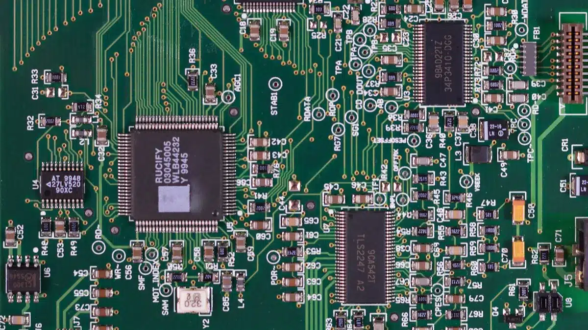
A printed circuit board (PCB) is very important in today’s electronics. It is a base that connects different electronic parts. This helps them work together well. A PCB usually has many layers. These layers include a substrate, pathways, and electronic parts.
Explain what a PCB is, including its structure and function.
The substrate is the base of the PCB. It gives support and keeps electricity from leaking. It is often made from materials like fiberglass or epoxy resin. On top of this base, there are pathways made of copper. These pathways connect different parts. They are etched into the copper layer. This creates a network for electrical signals to move between parts.
Electronic parts like resistors, capacitors, and integrated circuits are placed on the PCB. Each part has a special job in the circuit. For example, resistors limit current, capacitors store energy, and integrated circuits process signals. Together, these parts make a working electronic system.
A printed circuit board is like a layered sandwich. It has conductive and insulating layers. These layers have copper patterns that create traces and other features. They connect electronic parts. Components are usually soldered onto pads on the outer layers. This keeps them in place and connects them electrically.
Discuss its significance in electronic devices.
PCBs are very important for electronic devices to work. They give support, making sure parts stay in place while working. Also, PCBs connect parts electrically. They help distribute power and signals throughout the device.
The design of a PCB can change how well it works. For example, the thickness of the PCB affects how signals travel, how heat is managed, and how strong it is. Thicker boards can help with heat loss and reduce interference. This is important for keeping devices reliable.
Here are some key functions of PCBs in electronic devices:
They connect and wire parts through copper layers.
They distribute power and signals in the device.
They help remove heat from parts.
They allow parts to be placed with solder masks and silkscreens for protection.
These functions show why PCBs are the backbone of electronic circuits. Their role in making complex electronic functions possible makes them essential in modern electronic devices.
Components of Printed Circuit Boards

When you look at a printed circuit board (PCB), you will see some important parts that help it work. Two of the most important parts are traces and pads.
Traces and Pads
Traces are the copper paths that connect different parts on the PCB. They let electrical signals move between parts. The width and design of these traces can change how well the PCB works. Wider traces can carry more current with less resistance. This is important for delivering power efficiently.
Here’s a quick overview of how traces affect electrical performance:
Aspect | Description | Impact on Electrical Performance |
|---|---|---|
Traces | Copper paths connecting parts, designed with specific width, thickness, and layout. | Affect resistance, current capacity, signal quality, crosstalk, and EMI. Wider traces lower resistance and support higher currents; layout affects interference and heat management. |
Pads | Copper areas for soldering parts, available as through-hole or surface-mount types. | Provide strong electrical connections and good conductivity, which is important for reliable part attachment and signal flow. |
Copper is the main material for both traces and pads because it conducts electricity well and lasts a long time. It can handle the heat from soldering, making sure connections are reliable. However, new materials like graphene and conductive polymers are being developed. They offer special benefits for certain uses.
Vias and Layers
Vias are tiny paths that connect different layers of a multilayer PCB. They let signals and power move between layers, which is important for complex designs. Vias come in different types, like through-hole, blind, buried, and microvias. Each type has a special job, like saving space or improving signal quality.
The number of layers in a PCB affects how complex it is and its cost. More layers allow for more parts and better performance but raise manufacturing costs. Designers usually try to use the least number of layers needed to keep it working while controlling costs.
Types of PCBs
When you look into printed circuit boards (PCBs), you will see three main types: single-sided, double-sided, and multi-layer. Each type has special features and uses for different electronic needs.
Single-Sided
Single-sided PCBs have one copper layer on a base core, which is usually made from fiberglass. This design is simple and cheap. You can find these PCBs in devices like cameras, calculators, and printers. Here are some important points about single-sided PCBs:
Advantages:
They are great for low-density circuits.
Disadvantages:
They can pick up more electromagnetic interference (EMI).
Double-Sided
Double-sided PCBs have copper layers on both the top and bottom sides. This design allows for more complex circuits by connecting layers with vias. You will often see double-sided PCBs in things like car dashboards and industrial controls. Here are some key points:
Advantages:
They have more circuit space with two layers for connections.
They offer better performance and design options.
Disadvantages:
They cost more than single-sided PCBs.
They are harder to manufacture.
Multi-Layer
Multi-layer PCBs have three or more copper layers stuck together. This design supports high-density circuits and complex electronic functions. You will find multi-layer PCBs in advanced technology like smartphones and medical devices. Here are some features:
Advantages:
They work well with electromagnetic compatibility.
Disadvantages:
They are more expensive to make.
They have more complicated manufacturing steps.
Knowing the types of PCBs helps you pick the right one for your electronic projects. Each type has a specific use, making them important in modern technology.
Manufacturing Process of Printed Circuit Boards

Making a printed circuit board (PCB) has several important steps. You begin with design and prototyping. This sets up the whole PCB manufacturing process.
Design and Prototyping
In this stage, you make a detailed plan for your PCB. Here are the main steps in the PCB design and prototyping process:
Circuit Schematic Design: You draw the circuit plan and place parts on a virtual board.
Gerber File Generation: You save design files in Gerber format for making the PCB.
PCB Fabrication: This includes checking the design, preparing materials, imaging and etching, drilling, plating, applying solder mask and silkscreen, and testing electrically.
PCB Assembly: You put and solder parts using manual or automated methods like Surface Mount Technology (SMT).
Testing: You run electrical and functional tests to check board quality and performance.
During the design phase, you use special PCB design software. Some popular tools in 2025 are Altium Designer, Siemens PADS, and KiCAD. Each tool has unique features for different users, from hobbyists to big companies.
Software Tool | Key Features | Typical Users / Industries |
|---|---|---|
Altium Designer | Unified design workspace, advanced routing, 3D modeling, simulation, cloud collaboration | Aerospace, automotive, medical devices, consumer electronics |
Siemens PADS | Customizable layout, simulation, thermal analysis, mechanical CAD integration | Small/mid-size companies, high-speed digital design |
KiCAD | Free/open-source, schematic capture, PCB layout, 3D viewer, interactive routing, unlimited layers | Hobbyists, educators, small businesses |
Fabrication and Assembly
After you finish the design, the next step is fabrication. This process uses several techniques to create the physical PCB. Here are some common fabrication techniques:
Etching: This method removes extra copper, making the desired circuit pattern.
Drilling: You make holes for through-hole parts and vias using mechanical or laser drills.
Plating: This step adds copper inside drilled holes to connect layers electrically.
After fabrication, you go to assembly. This stage involves placing parts on the PCB and soldering them. Quality control is very important here. You can use different methods to ensure your assembled PCBs are reliable:
In-Circuit Testing (ICT): This checks how well parts work, finding shorts, opens, and wrong values.
Functional Testing: This simulates working conditions to check PCB functionality.
Standard Operating Procedures (SOPs): These make sure assembly processes are consistent.
The average time to make a standard PCB from design to assembly usually takes 2 to 8 weeks. This time can change based on complexity, volume, and technology used. For example, simple prototypes can be done in 1 to 3 weeks, while high-volume production may take longer.
Stage | Duration (working days) |
|---|---|
Bare PCB Manufacturing | 3–15 |
Component Procurement | Up to 17 |
PCB Assembly | 1–3 |
Packaging and Delivery | 1 |
Knowing the manufacturing process of PCBs helps you see the complexity and precision needed to create these important parts of modern electronics.
Applications of PCBs
Printed circuit boards (PCBs) are very important in many industries. You can find them in consumer electronics, cars, communication devices, and medical tools. Each area needs PCBs for different reasons.
In the consumer electronics field, PCBs are key parts of gadgets like smartphones, laptops, and gaming consoles. This area makes up about 34% of the global PCB market. As technology improves, the need for better electronics keeps growing.
The automotive industry is changing quickly. It is now the fastest-growing area for PCBs, with an expected growth rate of about 5% each year from 2023 to 2028. Electric vehicles (EVs) and advanced driver-assistance systems (ADAS) need high-quality PCBs. Here are some main uses of PCBs in cars:
PCBs help manage charging systems for electric vehicles, making sure power is delivered well.
They control how motors work and manage batteries in EVs.
PCBs support displays and navigation systems in vehicles.
In the telecommunications field, PCBs are needed for devices that help people communicate. This industry makes up about 30% of the PCB market. The growth of 5G networks and the Internet of Things (IoT) has raised the need for complex, high-quality PCBs. The market is expected to grow a lot due to new technology.
The medical device field also depends on PCBs. These boards make sure diagnostic and treatment devices are reliable and accurate. Medical PCBs must follow strict safety rules, which makes them very important for patient care. They allow for smaller designs and work with IoT for smart healthcare solutions.
PCBs are essential for modern technology. They make many devices you use every day work. As industries keep innovating, the need for PCBs will keep growing.
In conclusion, printed circuit boards (PCBs) are very important in today’s electronics. They give a strong base for connecting parts, allowing for smaller designs and better performance. As you have seen, PCBs are needed in many areas, like consumer electronics, cars, communication, and healthcare.
Looking forward, some trends will change PCB technology in the next few years:
High-Density Interconnect (HDI) PCBs will make smaller, stronger devices.
Flexible and rigid-flex PCBs will become popular for being light and adaptable.
Eco-friendly practices will push for sustainable manufacturing.
New materials will improve performance in high-frequency uses.
Smart PCBs will include sensors and processors for IoT and AI.
These changes will keep PCBs leading the way in technology innovation.
FAQ
What is the main purpose of a PCB?
A PCB connects electronic parts. This lets them work together and communicate. It gives a strong base for parts. This helps keep electrical connections reliable and signals moving efficiently.
How do I choose the right type of PCB?
Think about how complex your project is and how much space you need. Single-sided PCBs are good for simple designs. Double-sided and multi-layer PCBs are better for more complex circuits and higher density.
What materials are used in PCBs?
Common materials are fiberglass for the base and copper for traces and pads. Some advanced PCBs use materials like polyimide for flexibility or aluminum to help with heat.
Can I design my own PCB?
Yes, you can design your own PCB. You can use software like KiCAD or Altium Designer. These tools help you make schematics and layouts, making it easier to design.
How long does it take to manufacture a PCB?
The time to make a PCB depends on how complex it is and how many you need. Usually, it takes 2 to 8 weeks from design to assembly. Simple prototypes may take 1 to 3 weeks, while making a lot can take longer.
See Also
Understanding The Functionality And Importance Of PCBA Motherboards
The Role Of PCB Design And Its Significance In Electronics
Emerging Developments In PCB And PCBA Design And Manufacturing
Benefits And Obstacles Of Flex PCBA In Contemporary Electronics
Streamlined Approaches To Rapid PCBA For Electronics Projects
