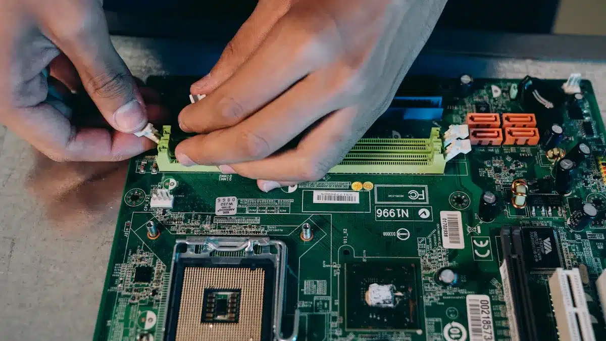
PCB production and assembly are two crucial steps in creating electronic devices. PCB production involves the fabrication of the bare printed circuit board (PCB), while PCB assembly focuses on placing and soldering components onto the board to ensure it functions properly. Understanding the process of pcb production and assembly is essential for anyone working in electronics, as these steps significantly impact the performance and quality of the final product.
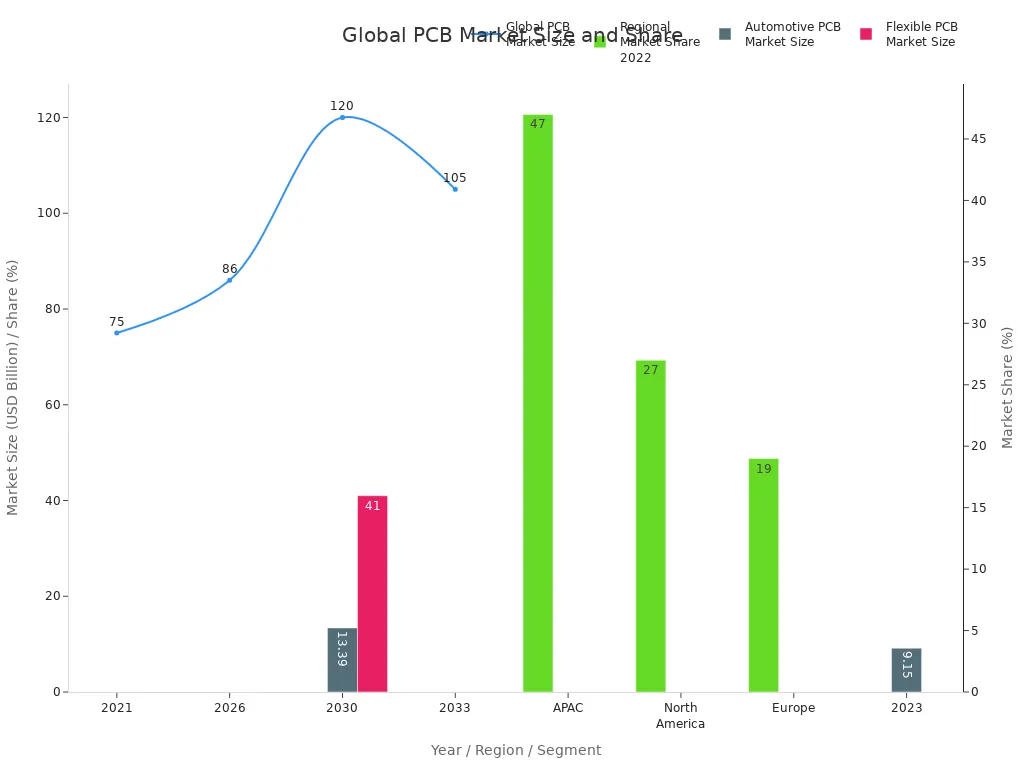
There are some common misconceptions about pcb production and assembly. For instance, some believe that component placement is arbitrary, but in truth, precise placement is vital for the board’s operation. With the global PCB market projected to reach $120 billion by 2030, having a clear understanding of pcb production and assembly has never been more important.
Key Takeaways
PCB fabrication makes the basic circuit board. It does this by layering materials and etching copper. PCB assembly adds and solders electronic parts onto the board. This makes the board work.
Both fabrication and assembly have important steps. These steps help ensure quality. They include choosing materials, drilling, applying solder paste, and inspecting.
Good design choices help both fabrication and assembly. They reduce mistakes, lower costs, and speed up production.
Knowing the time, cost, and challenges of each process helps you make better choices for your electronics projects.
Quality control and careful planning in both fabrication and assembly create reliable, long-lasting, and high-performing electronic devices.
PCB Fabrication
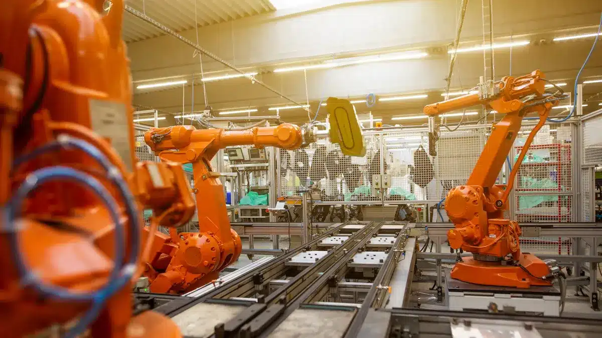
PCB fabrication is how we make the bare printed circuit board (PCB). This board is the base for electronic devices. This step is very important. It affects the quality and reliability of the final product. Knowing the key steps in PCB fabrication helps you see how these processes improve the performance of electronic devices.
Key Steps in Fabrication
The PCB fabrication process has several important steps. Here’s a list of the standard procedures involved:
Receiving Customer Files: Manufacturers check files like Gerber or IPC-2581 to get ready for production.
Material Selection and Stackup: Engineers pick base materials like laminates and copper foil, deciding the layer stackup.
Inner-layer Processing: This includes cleaning, applying photoresist, UV exposure, developing, etching, and stripping to make inner copper patterns.
Lamination: Layers are stacked and pressed with heat and pressure to bond into a multilayer board.
Drilling: Precise drilling makes vias and holes, then cleaning removes any resin smear.
Copper Plating: Electroless and electrolytic copper plating add copper inside holes and on surfaces.
Outer-layer Processing: Like inner-layer processing, this step includes photoresist application, exposure, developing, and etching for outer copper patterns.
Solder Mask Application: A liquid solder mask is put on to protect copper and vias from solder.
Silkscreen Printing: Text and symbols are printed on the board surface for identification.
Final Inspection and Testing: Dimensional checks, electrical tests, and visual inspections ensure quality before shipping.
These steps are the backbone of the PCB manufacturing process. They make sure the circuit board meets the required specifications and standards.
Importance of PCB Fabrication
The importance of PCB fabrication is very high. Good fabrication affects the reliability and performance of electronic devices. Here are some key reasons why PCB fabrication matters:
Signal Integrity: Proper fabrication keeps signal integrity by reducing electromagnetic interference and crosstalk.
Thermal Management: Good thermal management during fabrication stops overheating, which helps components last longer.
Error Minimization: Accurate component placement lowers errors that could cause malfunctions.
Durability: A well-made PCB can handle environmental stresses, which is important for automotive and aerospace uses.
Also, new ideas in PCB fabrication, like using advanced materials and automation, improve production efficiency and product quality. As technology changes, staying updated on these advancements will help you make better choices in electronics manufacturing.
PCB Assembly
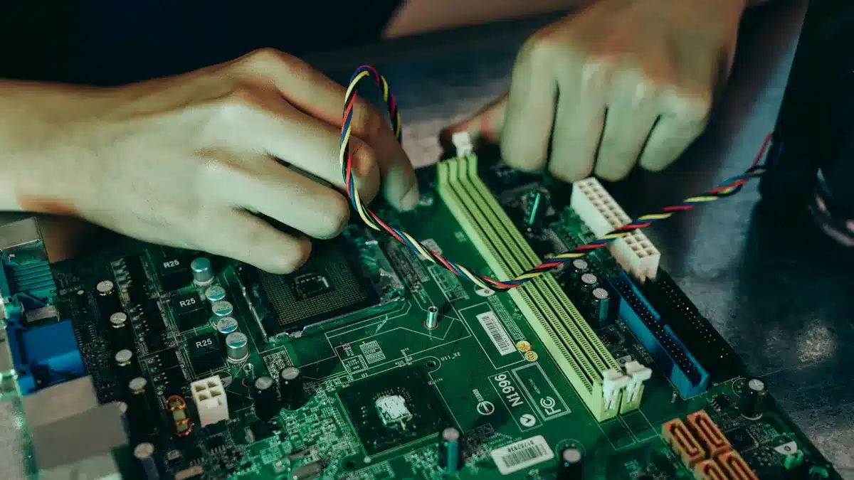
PCB assembly is how we turn a bare printed circuit board into a working electronic device. This step is very important. It involves placing and soldering parts onto the PCB. This allows the board to do its job. Knowing the key steps in the PCB assembly process helps you see how each part affects the quality and reliability of the final product.
Key Steps in Assembly
The PCB assembly process has several important steps. Here’s a list of the main procedures involved:
Design for Manufacturability (DFM) Check: Look over the PCB design to find any issues.
Solder Paste Application: Spread solder paste on the PCB pads using stencils for even coverage.
Pick and Place: Use machines to place surface mount technology (SMT) parts accurately on the PCB.
Reflow Soldering: Move the board through an oven to melt the solder paste, holding the parts in place.
Through-Hole Component Insertion: Put through-hole parts in by hand or with machines, then solder them.
Inspection: Do visual and machine checks to confirm part placement and solder quality.
Functional Testing: Run tests to make sure the assembled PCB works right and meets specifications.
Final Packaging: Get the assembled PCB ready for shipping, making sure it is safe from damage.
These steps are crucial for making sure the PCB assembly meets the needed standards for performance and reliability.
Importance of PCB Assembly
The importance of PCB assembly is very high. It greatly affects how well electronic devices work. Here are some key reasons why PCB assembly is so important:
Reliable Electrical Connections: Good assembly makes sure all parts are connected well, which is vital for device operation.
Miniaturization: New assembly methods allow for smaller designs, fitting more functions in less space.
Quality Control: Strict inspection during assembly helps find problems early, lowering the chance of failures in the final product.
Complex Circuitry Integration: PCB assembly helps combine complex circuits needed for modern electronics, improving device abilities.
Innovation and Efficiency: The assembly process encourages new ideas in manufacturing, leading to smaller, stronger, and more reliable products.
By understanding the importance of PCB assembly, you can see how it helps the success of electronic manufacturing.
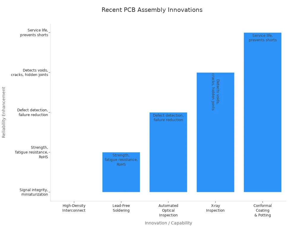
Comparing PCB Production and Assembly
When you look at PCB production and assembly, you see big differences in time, costs, and problems. Knowing these differences helps you make better choices for your projects.
Timeframes
The time needed for PCB fabrication and assembly changes based on how complex they are. Here’s a quick look at usual lead times:
PCB Fabrication Step | Time Duration |
|---|---|
Simple PCB total lead time | |
Moderate complexity PCB | 2-4 weeks |
Complex/high volume PCB | 4-8 weeks or more |
PCB Assembly Complexity | Lead Time |
|---|---|
Simple boards | |
Typical small prototype | 3-5 days |
Very complex designs | 10 days or more |
Things like design complexity and part availability can change these times. For example, designs with many layers or hard-to-find parts can cause delays.
Cost Considerations
Cost is very important in both PCB fabrication and assembly. Here’s a breakdown of usual costs:
PCB Fabrication Components | PCB Assembly Components | |
|---|---|---|
Materials | Substrate (like FR-4), Copper Thickness, Solder Mask | Parts (BOM variety, brand/type, buying sources) |
Process Costs | Layer count, Trace width/spacing, Drill and via types | Assembly labor and methods (SMT, THT, mixed assembly), soldering, checking, testing |
Quantity/Batch Effects | Board size, Panelization, Order volume (prototype vs mass production) | Volume effects on labor and buying costs |
PCB fabrication costs usually come from raw materials and how complex the manufacturing is. On the other hand, PCB assembly costs mainly come from buying parts and labor-intensive work.
Common Challenges
Both PCB fabrication and assembly have common challenges. Here are some common problems:
Challenge | Description | How It Is Addressed |
|---|---|---|
Design Flaws | Problems like wrong component placement and bad thermal management | Use Design for Manufacturability (DFM) and do simulation/testing |
Component Placement | Misplacement causing shorts or board failure | Use automated pick-and-place machines and do regular checks |
Soldering Defects | Cold joints or not enough solder | Use proper soldering methods and high-quality materials |
By knowing these challenges, you can take steps to reduce risks in your PCB production and assembly processes.
Design Influence on PCB Processes
Design is very important in both PCB fabrication and assembly. The choices you make in design can greatly affect how well these processes work. Knowing how design impacts fabrication and assembly helps you make better PCBs.
Design and Fabrication
When you create a PCB, think about how its complexity affects fabrication. More complex designs usually need extra steps, special tools, and skilled workers. For example, using High-Density Interconnect (HDI) technology allows for smaller designs but raises manufacturing costs. To avoid expensive mistakes, use design rule checks (DRC) that fit your fabricator’s abilities. Here are some key points to keep in mind:
Trace and Space Tightness: Closer spacing makes etching harder and costs more.
Hole Size and Quantity: Smaller holes need precise tools, which takes more time and money.
Controlled Impedance: Needs special materials and exact trace width, making it more complex.
By following DFM guidelines, you can reduce redesigns and improve yield. Finding design problems early with DRC helps you avoid costly rework.
Design and Assembly
Your design choices also have a big effect on the assembly process. Smart component placement helps with smooth automated assembly and cuts down on production issues. Here are some best practices to improve assembly:
Proper Component Orientation: Align similar parts in the same direction to speed up placement.
Grouping Components: Place related parts close together to shorten trace lengths and lower signal interference.
Thermal Management: Put heat-producing parts in the center to keep airflow steady and avoid hotspots.
Also, planning your PCB layout before placing components helps optimize routing paths and reduce mistakes. By following these tips, you can make the assembly process more efficient and improve the overall quality of your PCB manufacturing.
In conclusion, knowing the differences between PCB assembly and fabrication is very important for making electronics. Here are the main differences:
Aspect | PCB Fabrication | PCB Assembly |
|---|---|---|
Definition | Making the bare board by layering materials and etching copper lines. | Attaching and soldering electronic parts onto the made board. |
Skill Requirements | Skills in materials science and precise machining are needed. | Understanding circuit design and soldering methods is necessary. |
Timeframes | Usually takes 3 to 7 days based on how complex it is. | Takes a similar time but can change depending on part availability. |
Cost Structure | Higher initial costs because of raw materials and setup fees. | Costs go up with larger orders due to labor and buying parts. |
By understanding these differences, you can make smart choices based on your project’s size and complexity. Think about your specific needs when deciding between assembly and fabrication services. This knowledge will help you improve production times, control costs, and ensure your product works well.
Keep in mind, making the right choice can greatly affect your project’s success!
FAQ
What is the difference between PCB fabrication and assembly?
PCB fabrication makes the bare circuit board. Assembly puts and solders parts onto that board. Both steps are important for making working electronic devices.
How long does PCB fabrication take?
PCB fabrication usually takes 1 to 8 weeks. This depends on how complex the design is. Simple boards may take 1-2 weeks, while complex designs can take longer.
What factors affect PCB assembly costs?
PCB assembly costs depend on part prices, labor, and how complicated the assembly is. Bigger orders can lower costs because of economies of scale.
Can I use the same design for both fabrication and assembly?
You should adjust your design for each process. Design for manufacturability (DFM) helps make sure your PCB works for both fabrication and assembly.
Why is quality control important in PCB processes?
Quality control makes sure that both fabrication and assembly follow industry standards. It helps stop defects, lowers failures, and boosts the overall reliability of electronic devices.
See Also
A Comprehensive Guide To PCBA Production And Assembly
Key Distinctions Between PCB And PCBA In Electronics
Unveiling The Lesser-Known Variations Between PCBA And PCB
Analyzing Functional And Structural Contrasts Of PCBA Versus PCB